


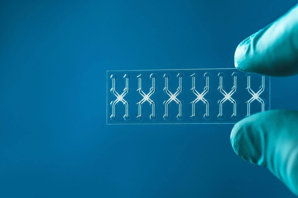
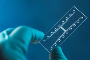
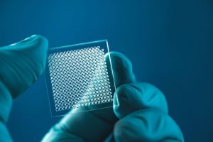
Responding to increasing customers’ needs, WOP has focused on glass microfluidic chip manufacturing with the objective to achieve the best features possible, thus increasing precision to the maximum.
While talking of microfluidics, GLASS, compared to other materials, offers a unique set of features. It is optically transparent, solid, electrically insulating, amorphous, has thermal stability and temperature resistance, chemical inertness to many fluids, biocompatibility, not permeable to gas. All this makes glass an ideal material for microfluidic devices.
And yet, it is not widely selected because conventional manufacturing of glass microfluidic devices is a complex, multi-step process that is not effective nor competitive.
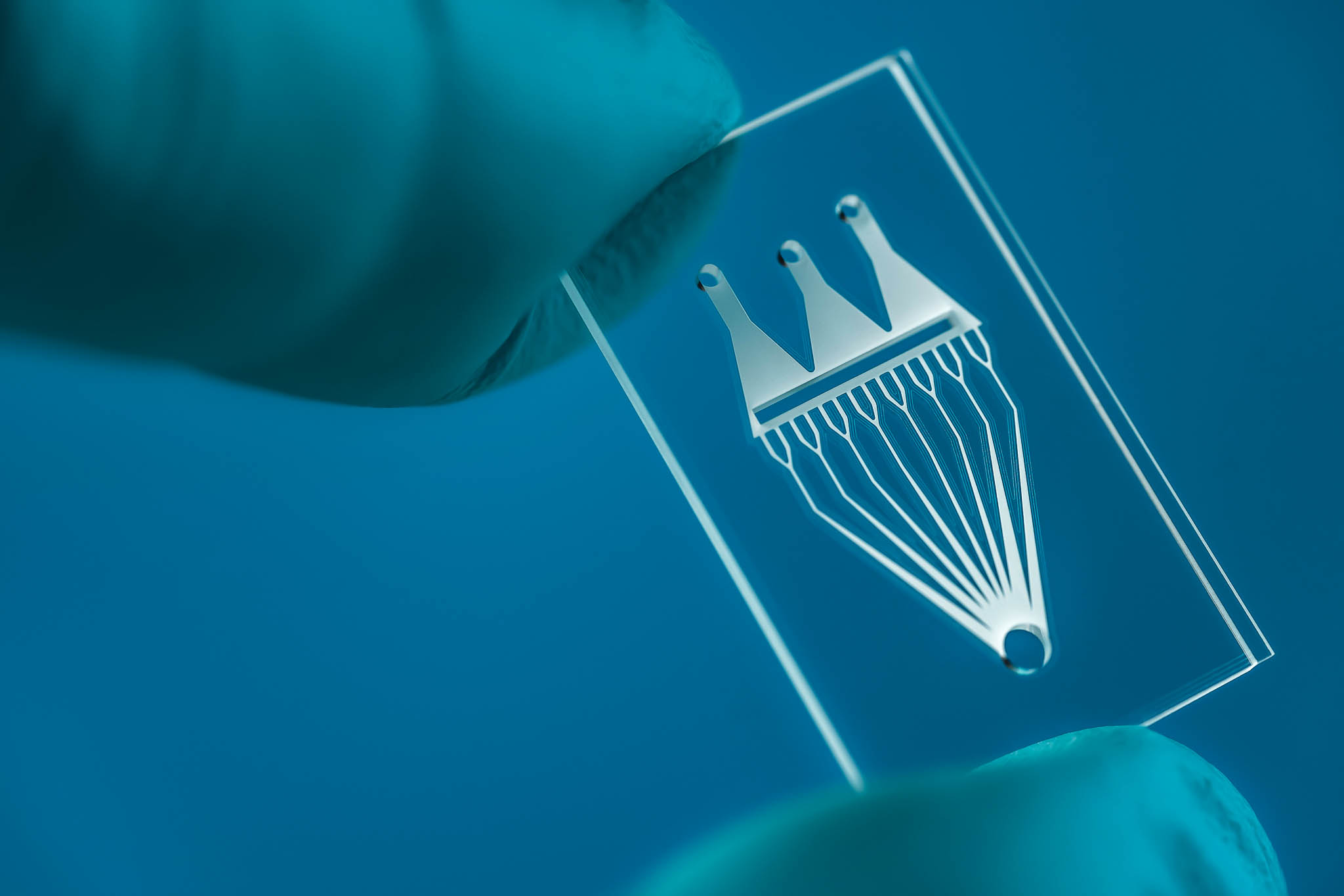
What we offer is a revolutionary glass processing technology that solves all conventional method limitations, thus allowing the micro-device industry to choose glass as the key material.
We offer droplet-based microfluidics, microfluidics for point-of-care, single-cell analysis, or any other custom application.
Microfluidic chip manufacturing
Microfluidic chip manufacturing

Microfluidic chips manufacturing

Overall, femtosecond laser micromachining of transparent materials (the one we use) provides many advantages over conventional methods and is ideally suited for the fabrication of microfluidic devices, especially glass ones.
The results, achieved using FemtoFBG present the stabilization of blue multi-emitter modules using fiber Bragg…
This EU-funded project is expected to revolutionize Green Energy Generation from photovoltaic panels across Europe.
WOP participates in the BILASURF project – a new European initiative to develop a solution…