


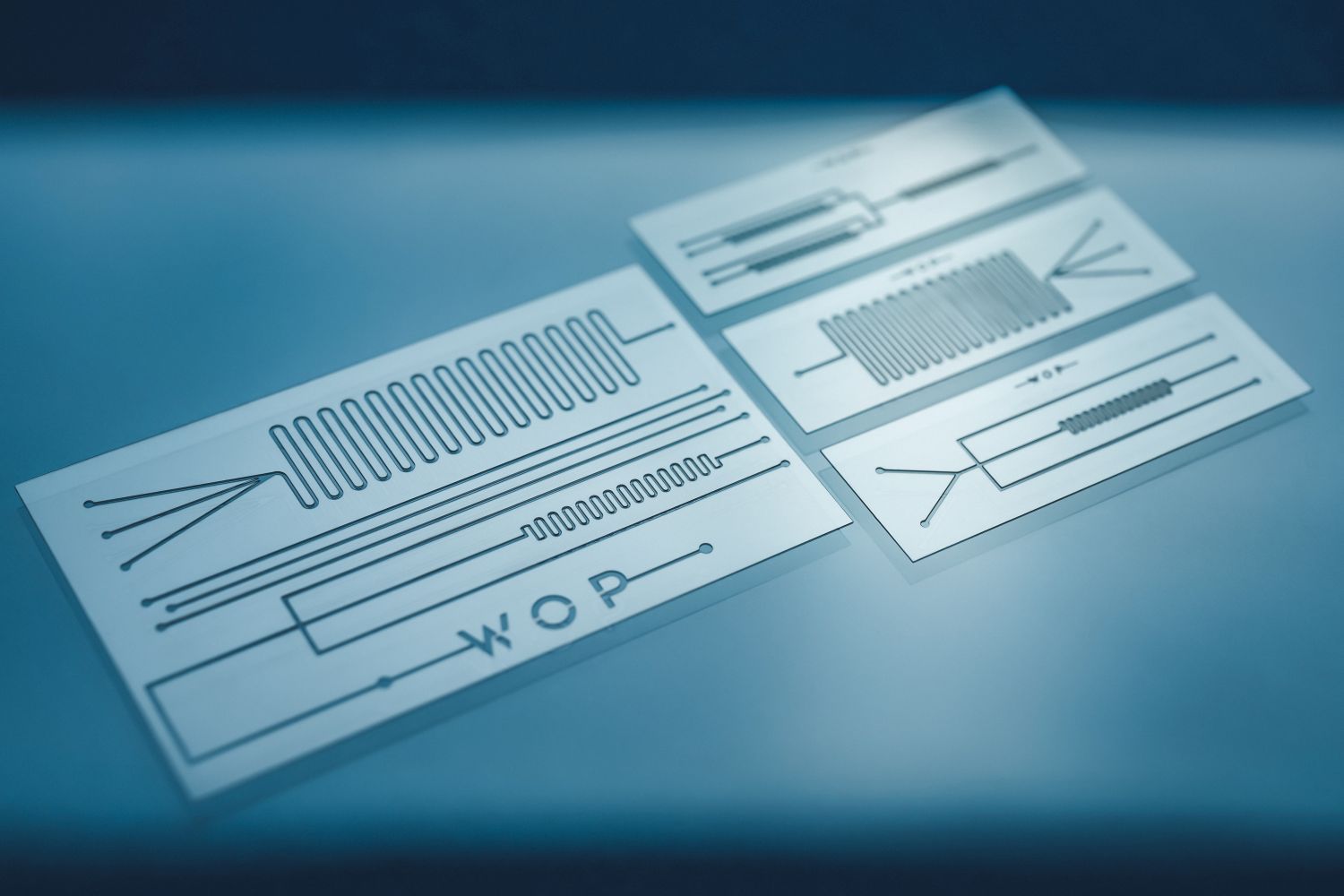
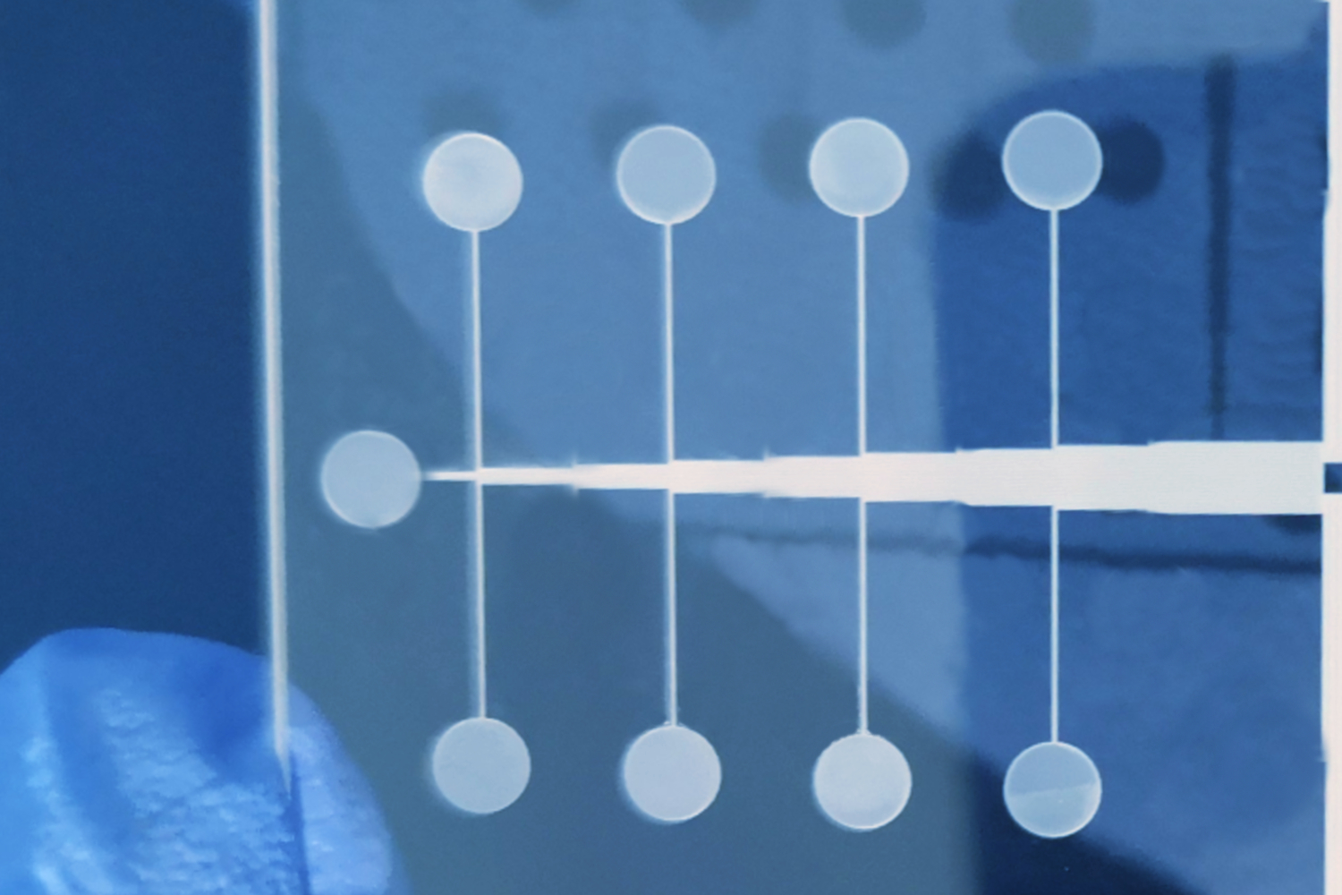
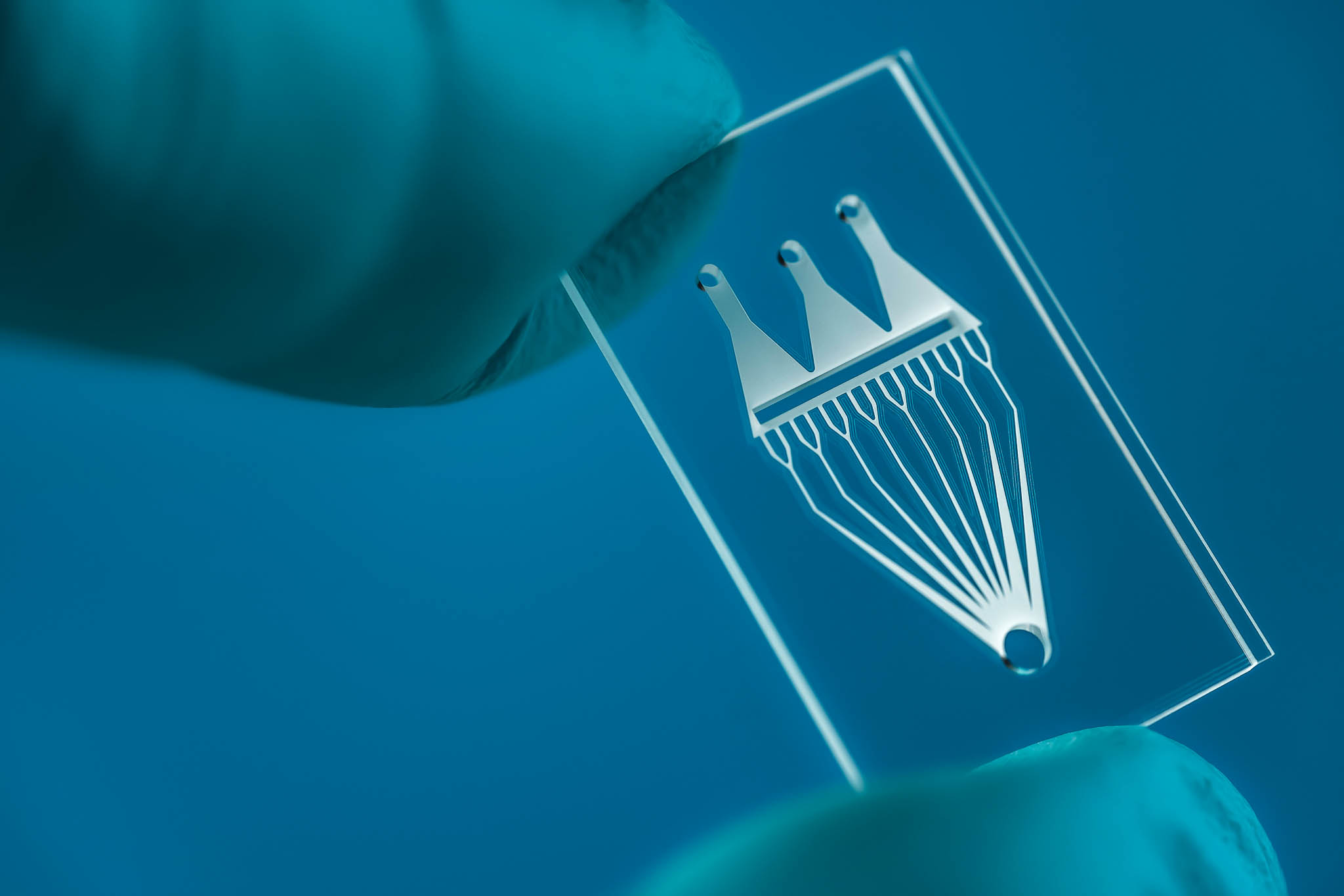
Microfluidic devices are applied in many fields, such as cell analysis, point of care, cell biology, chemical composition analysis, etc.
We offer ultra-high precision results in glass microfluidics. There is also a possibility to investigate other materials like silicon and polymers (PDMS). As every material has its advantages – the choice depends on the application, type of solvents, design, and budget.
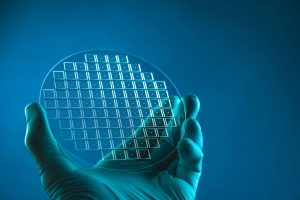
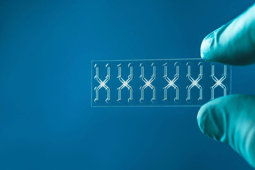
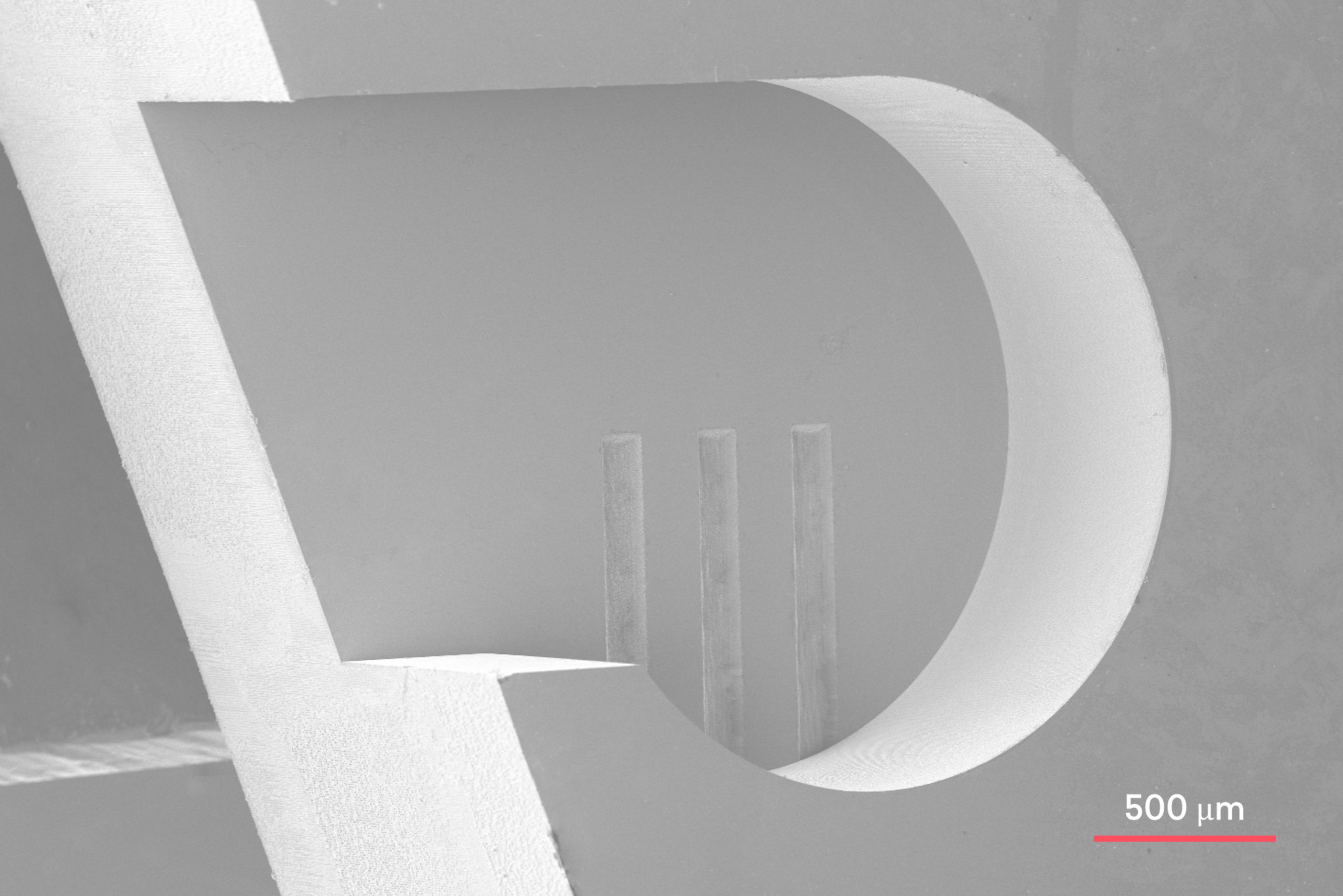
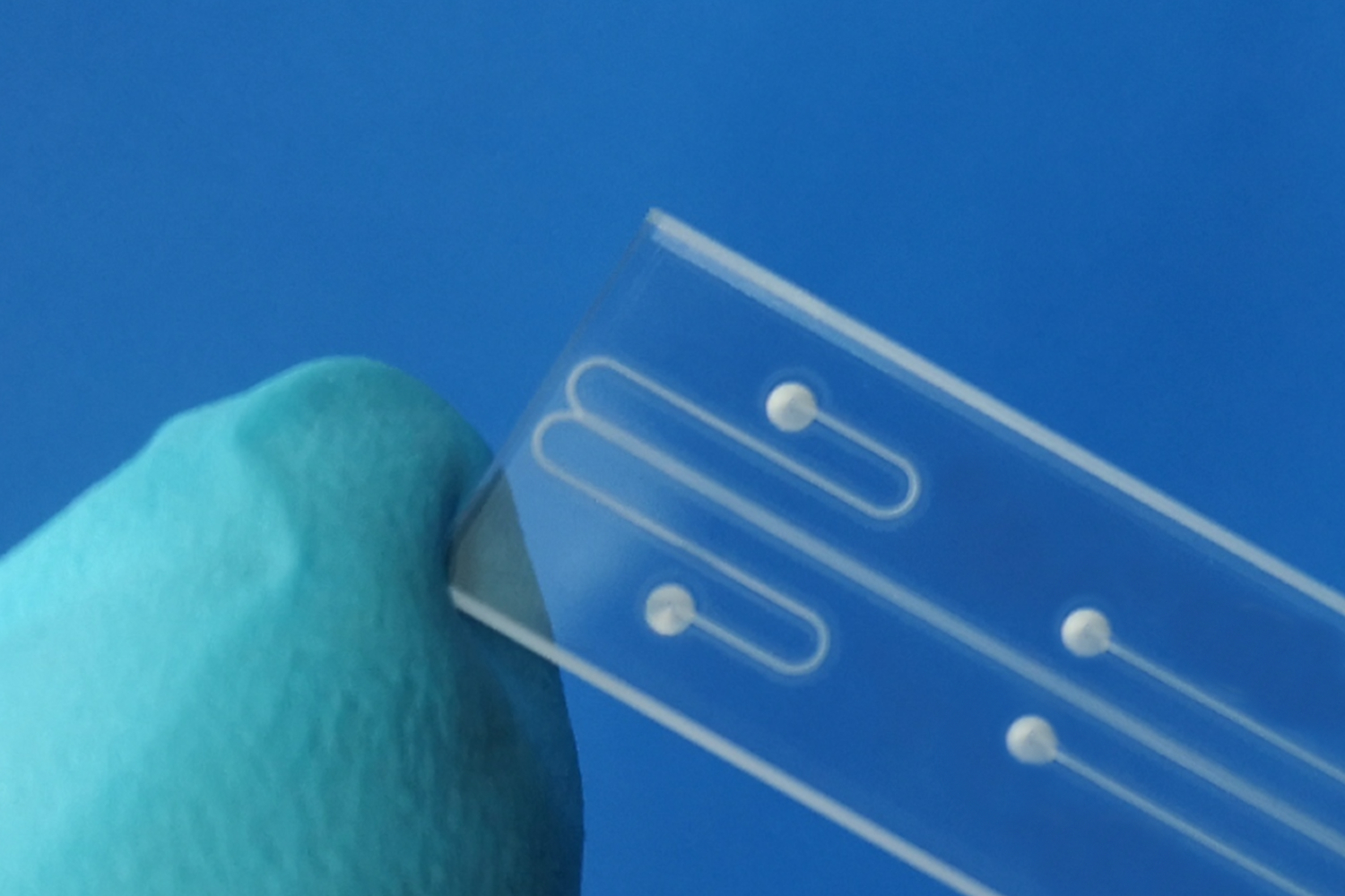
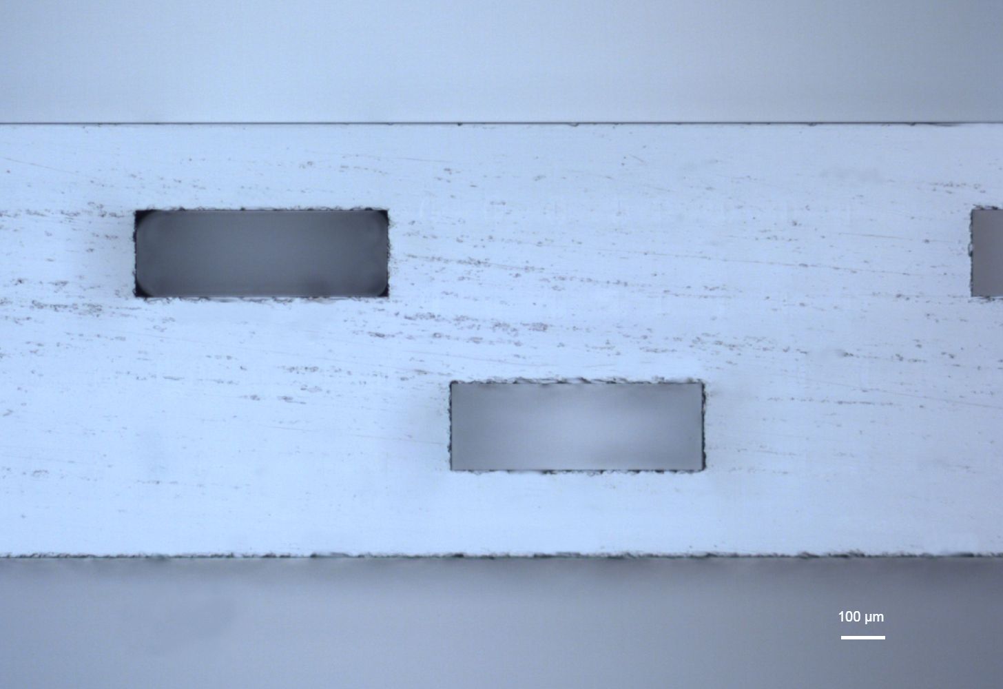
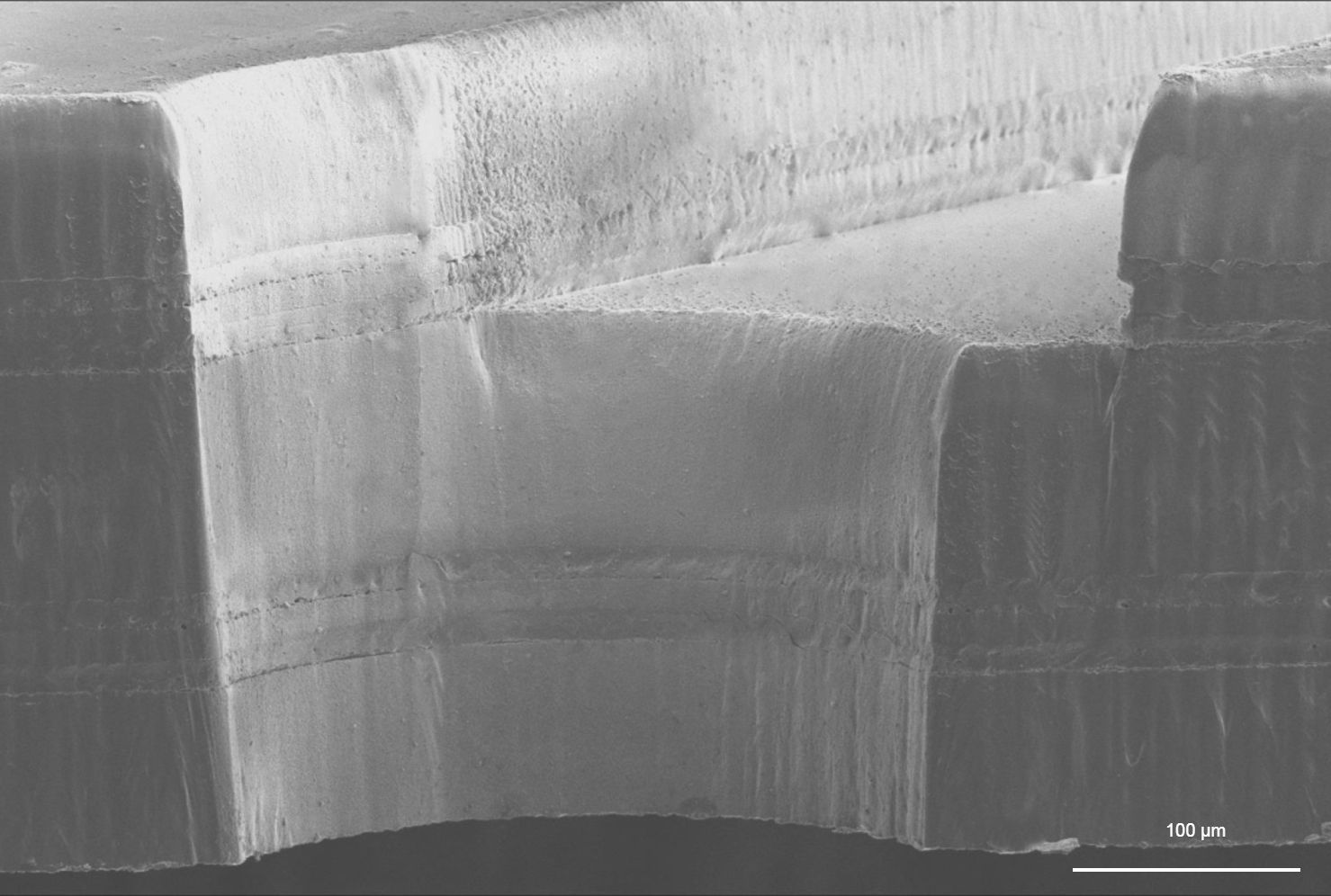
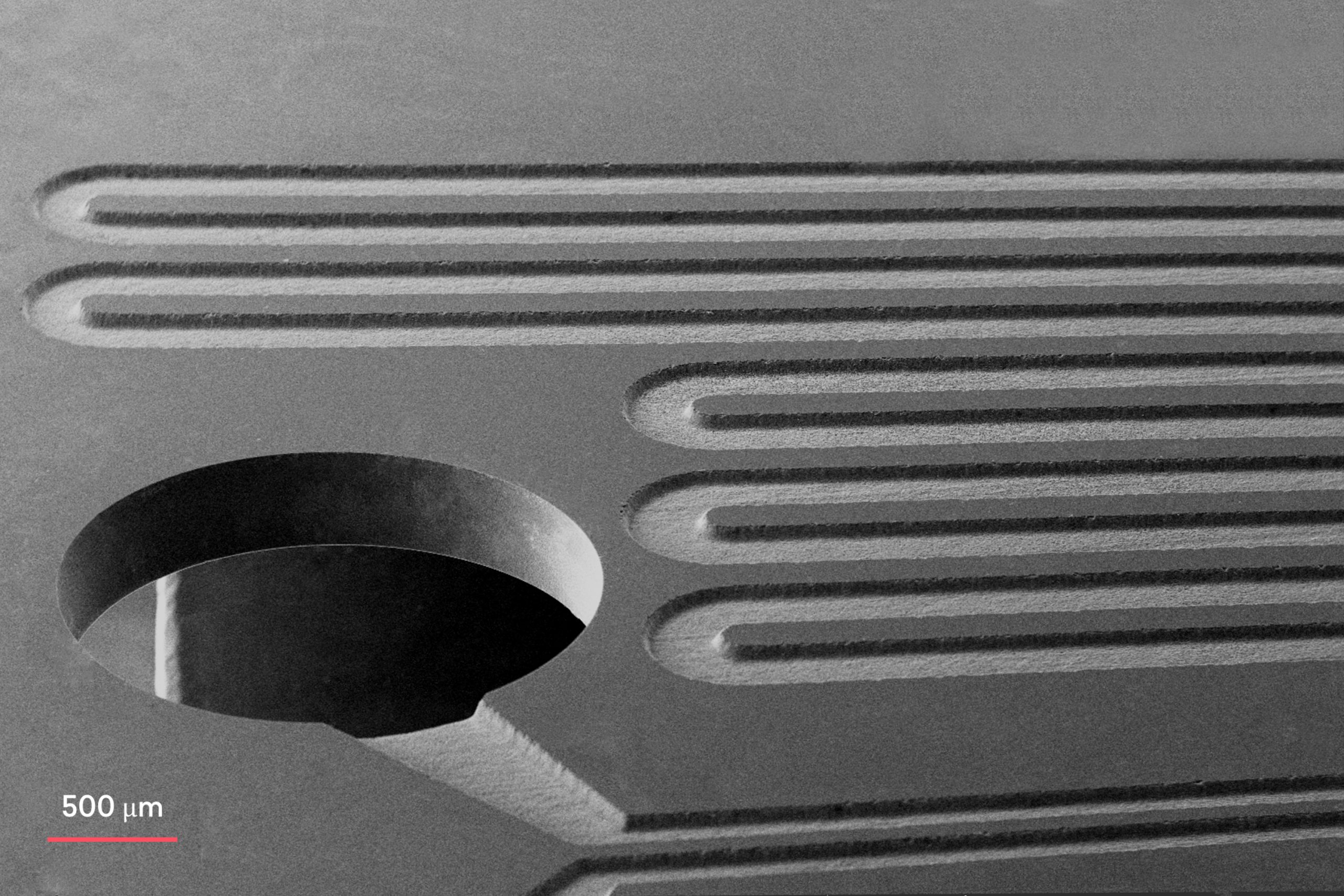
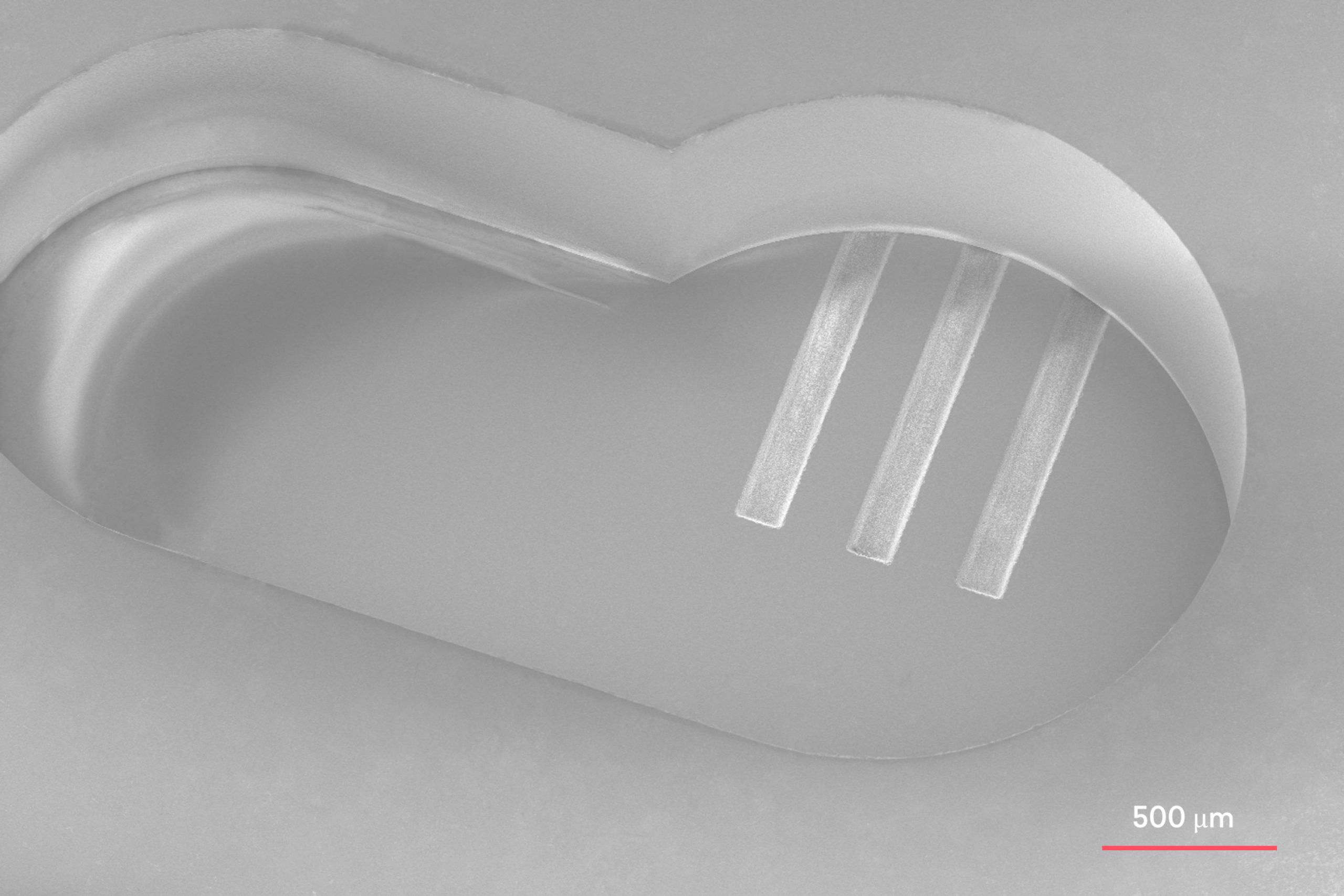
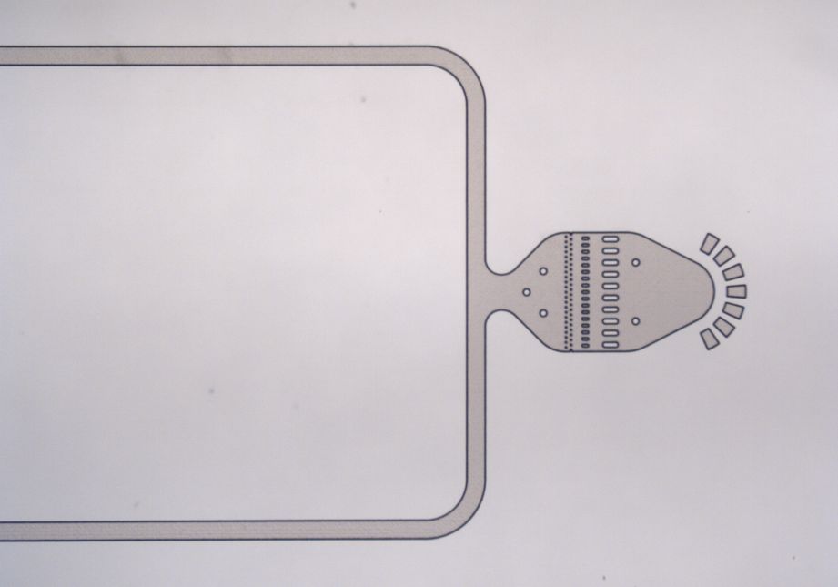
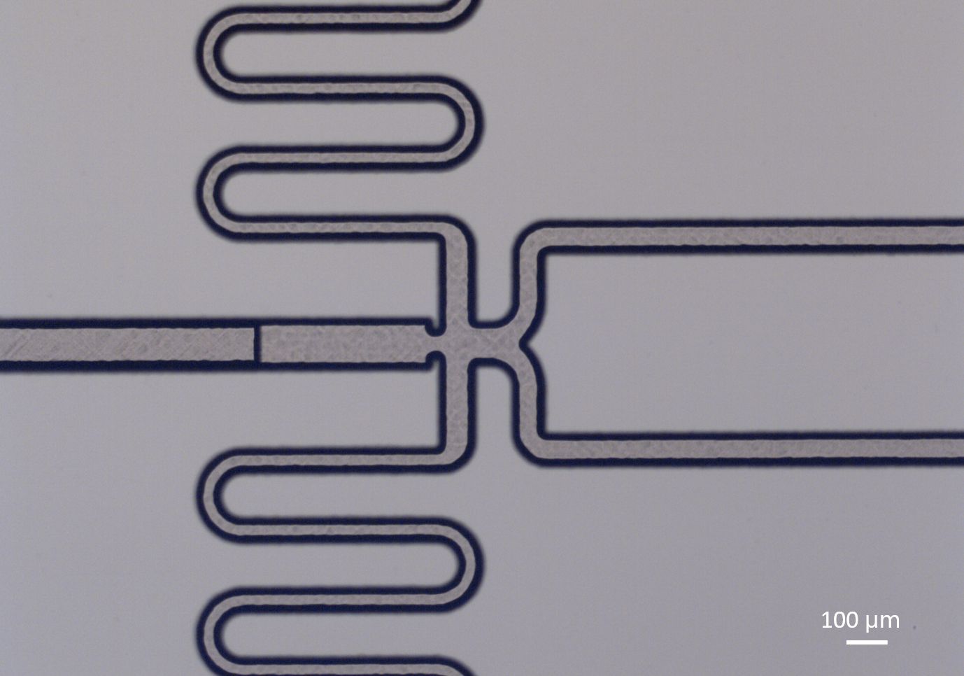
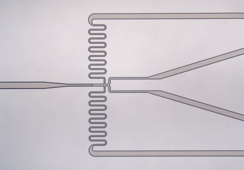
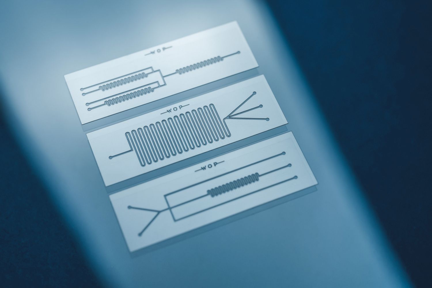
Wafer-level microfluidics fabrication
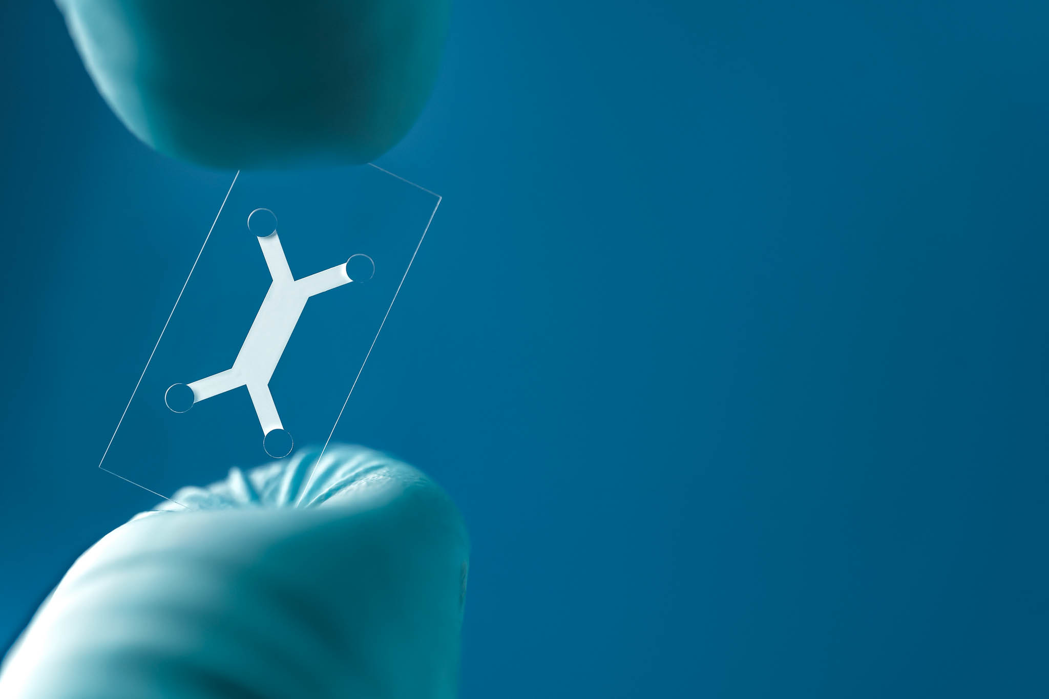
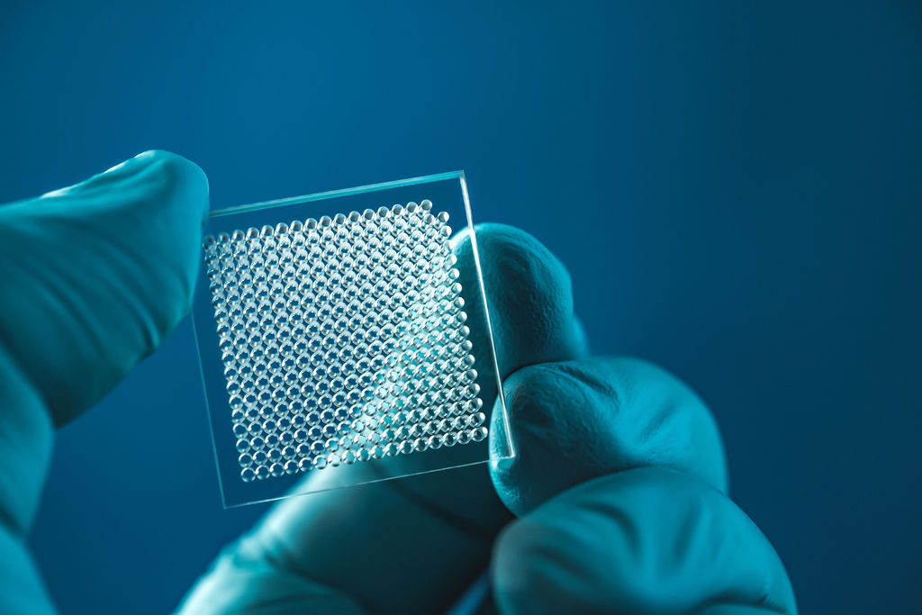
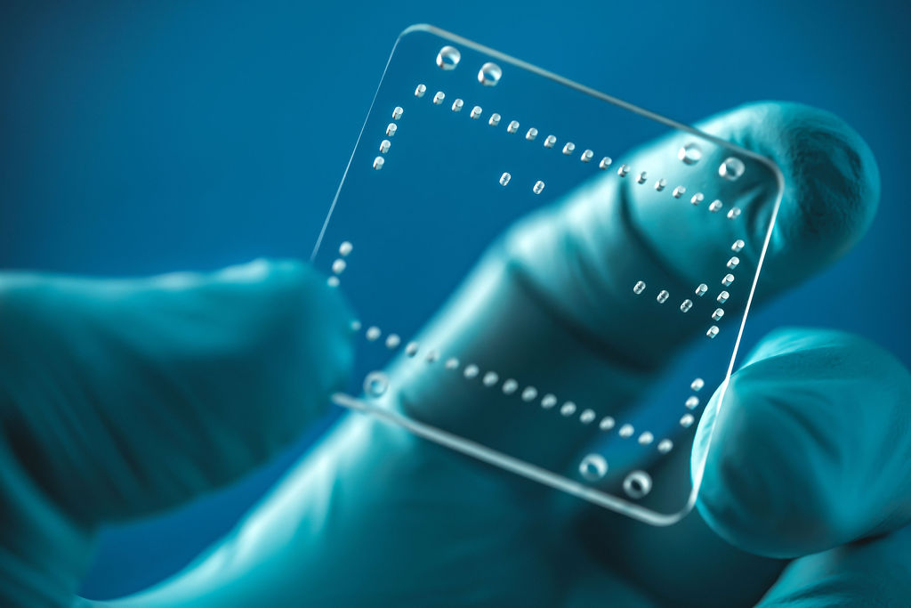
While talking of microfluidics, GLASS, compared to other materials, offers a unique set of features. It is optically transparent, solid, electrically insulating, amorphous, has thermal stability and temperature resistance, chemical inertness to many fluids, biocompatibility, and is not permeable to gas. All this makes glass an ideal material for microfluidic devices.
Yet, it is not widely selected because conventional manufacturing of glass microfluidic devices is a complex, multi-step process that is not effective nor competitive.
We offer a revolutionary glass processing technology that solves all conventional method limitations, thus allowing the micro-device industry to choose glass as the key material.
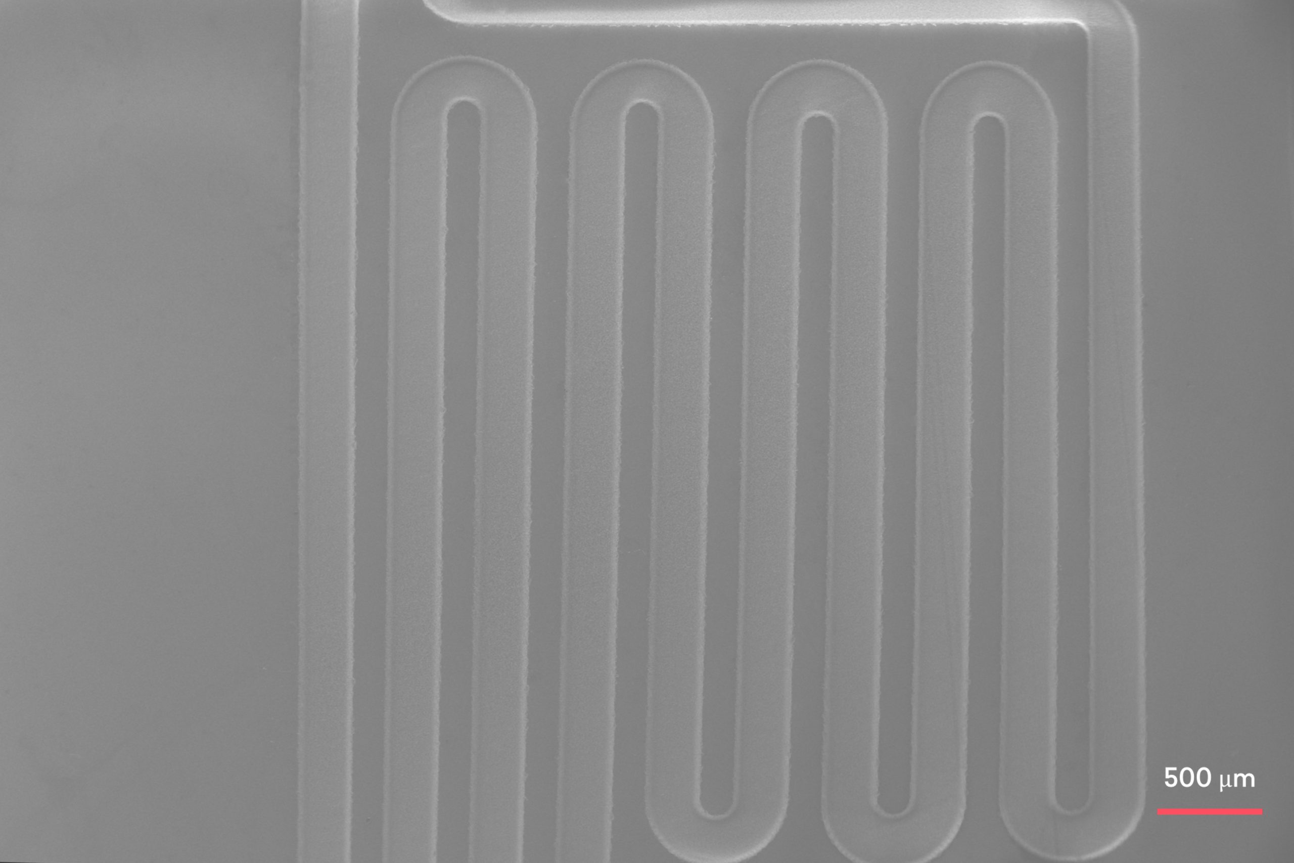
Our technology is ultra-fast, cost-efficient, and ultra-precise, offering exceptional precision and quality results on glass.
Glass multiwell plates designed to exact cell culture application. Circular wells, square wells, hexagon wells,…
We ensure ultra-high precision and quality tempered and non-tempered glass laser cutting and dicing –…
Glass & sapphire cutting and dicing workstation for industry, that outperforms other glass cutting methods.
Mesh filters manufacturing – custom design, diverse materials, µm sizes, rapid prototyping.
Rapid prototyping services to test your idea in an actual environment.
Ultra-high precision production services on all materials - glass, sapphire, ceramics, silicon, optical fibers, metal, plastic.
Tailor-made laser systems for industry & science. Designed for your specific applications.
WORKSHOP OF PHOTONICS
Mokslininku st. 6A, Vilnius, LT-08412, Lithuania
Phone: +370 5 215 7551
E-mail: [email protected]
Altechna R&D, UAB
Company code 301502628
VAT code LT100006155012
Bank – SEB 70440
LT87 7044 0600 0770 8092


