


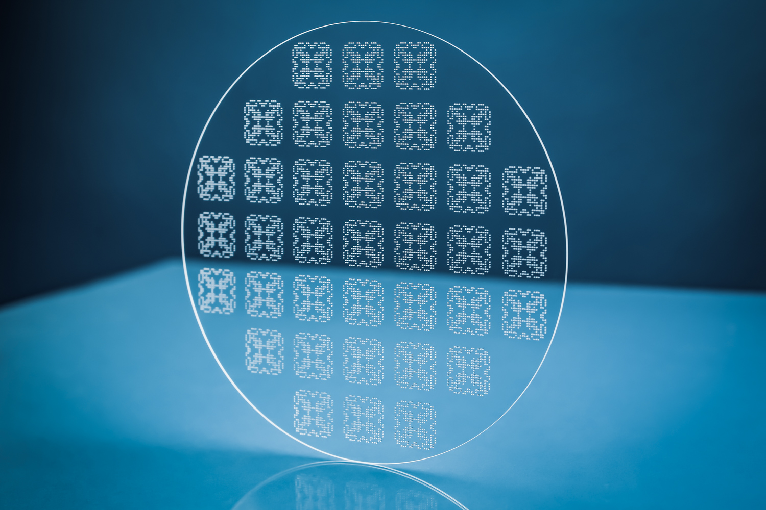
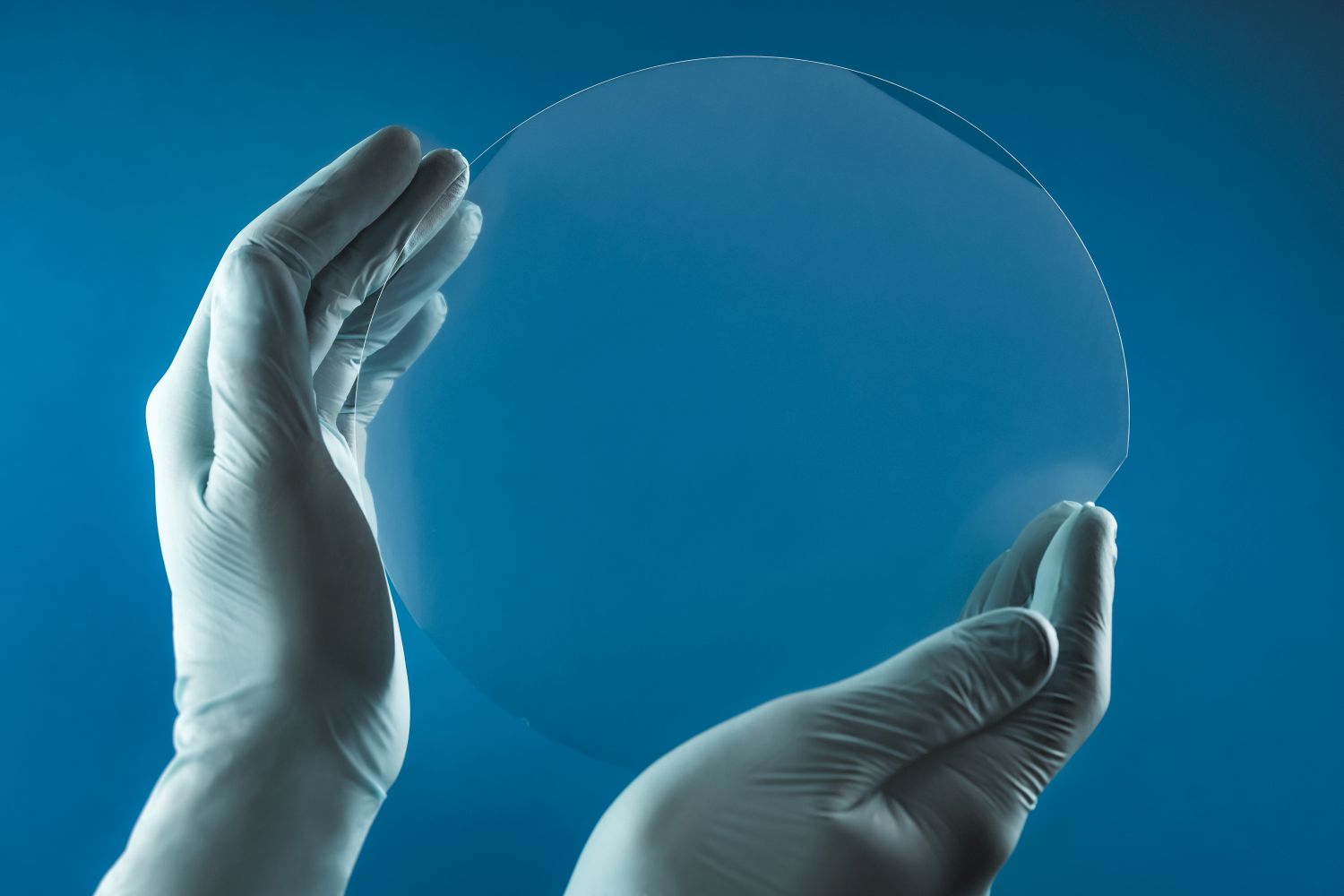
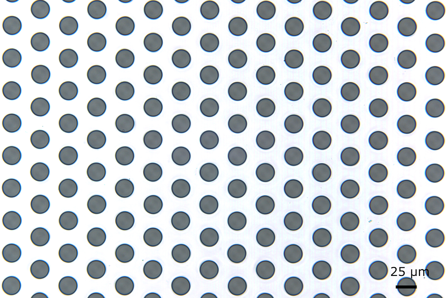
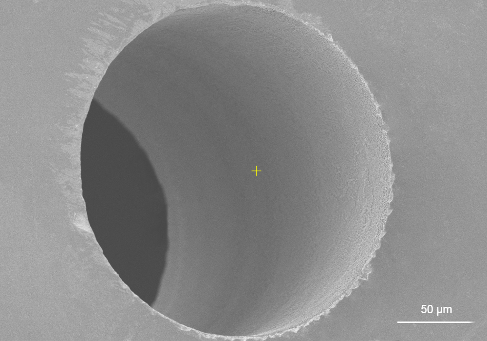
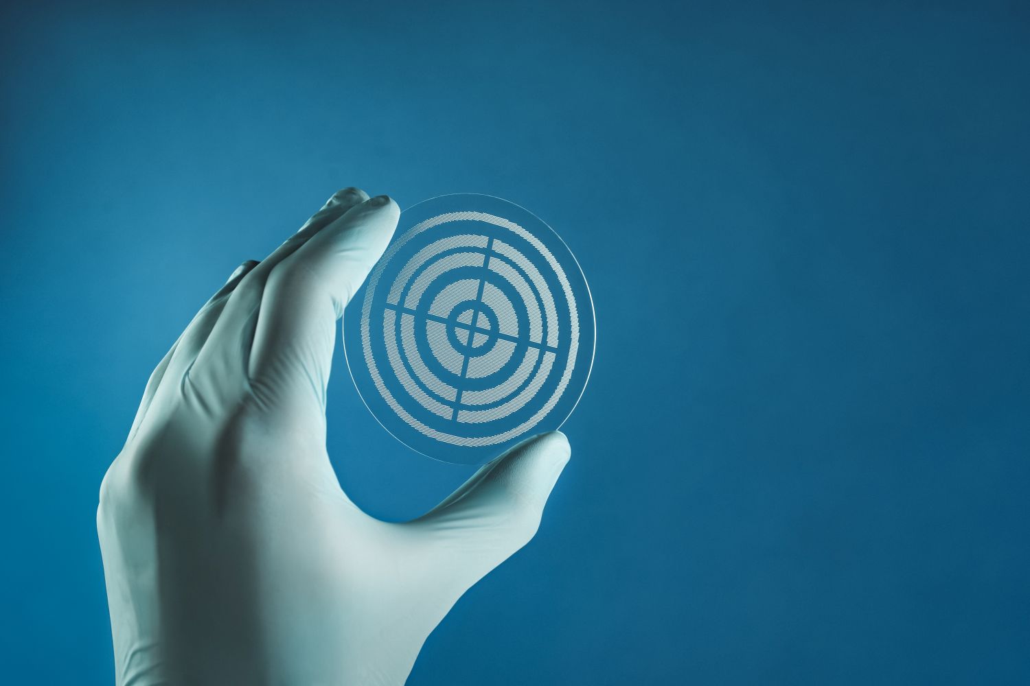
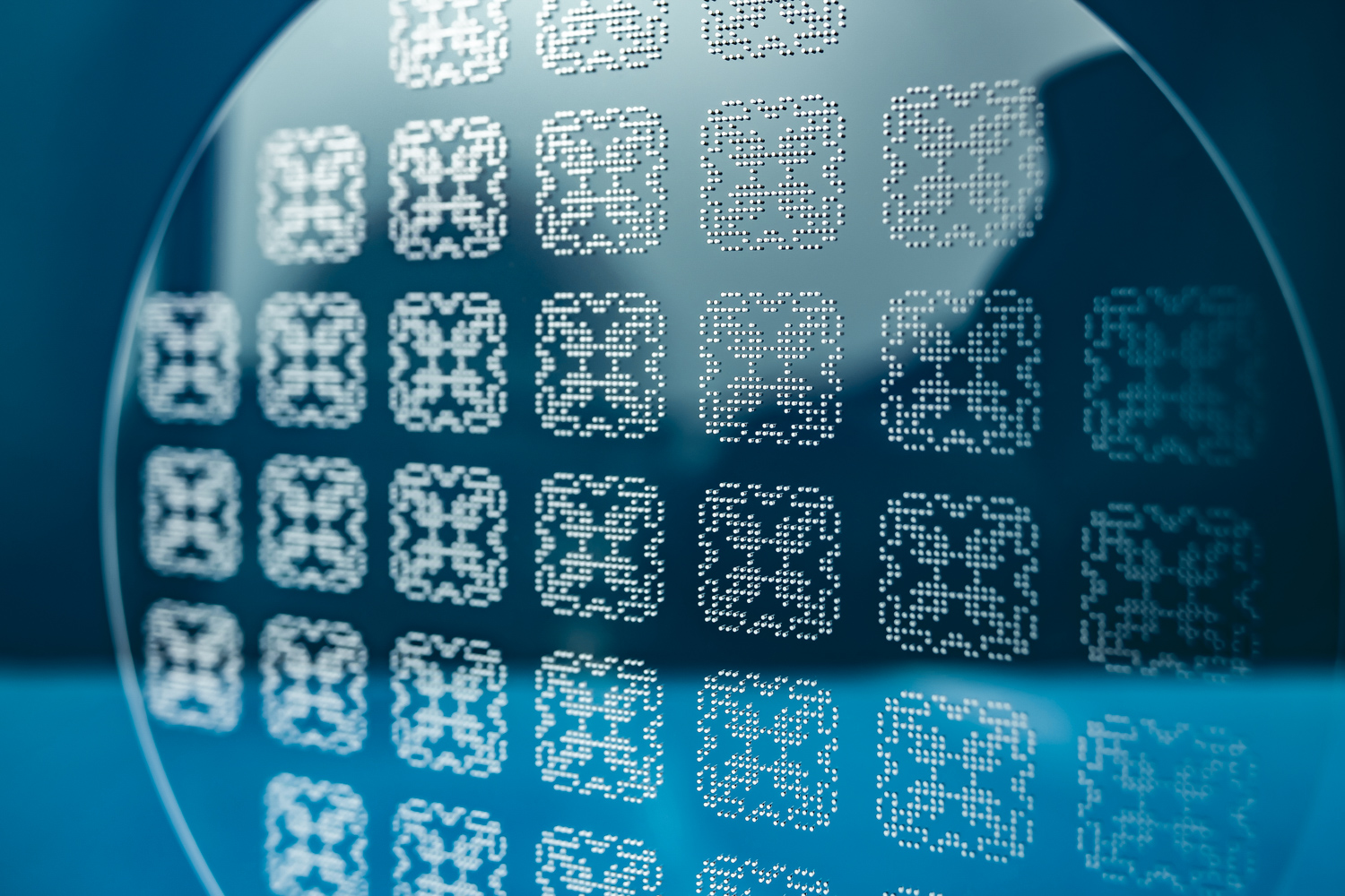
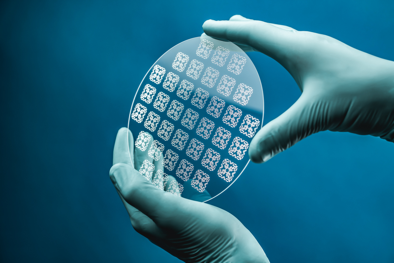
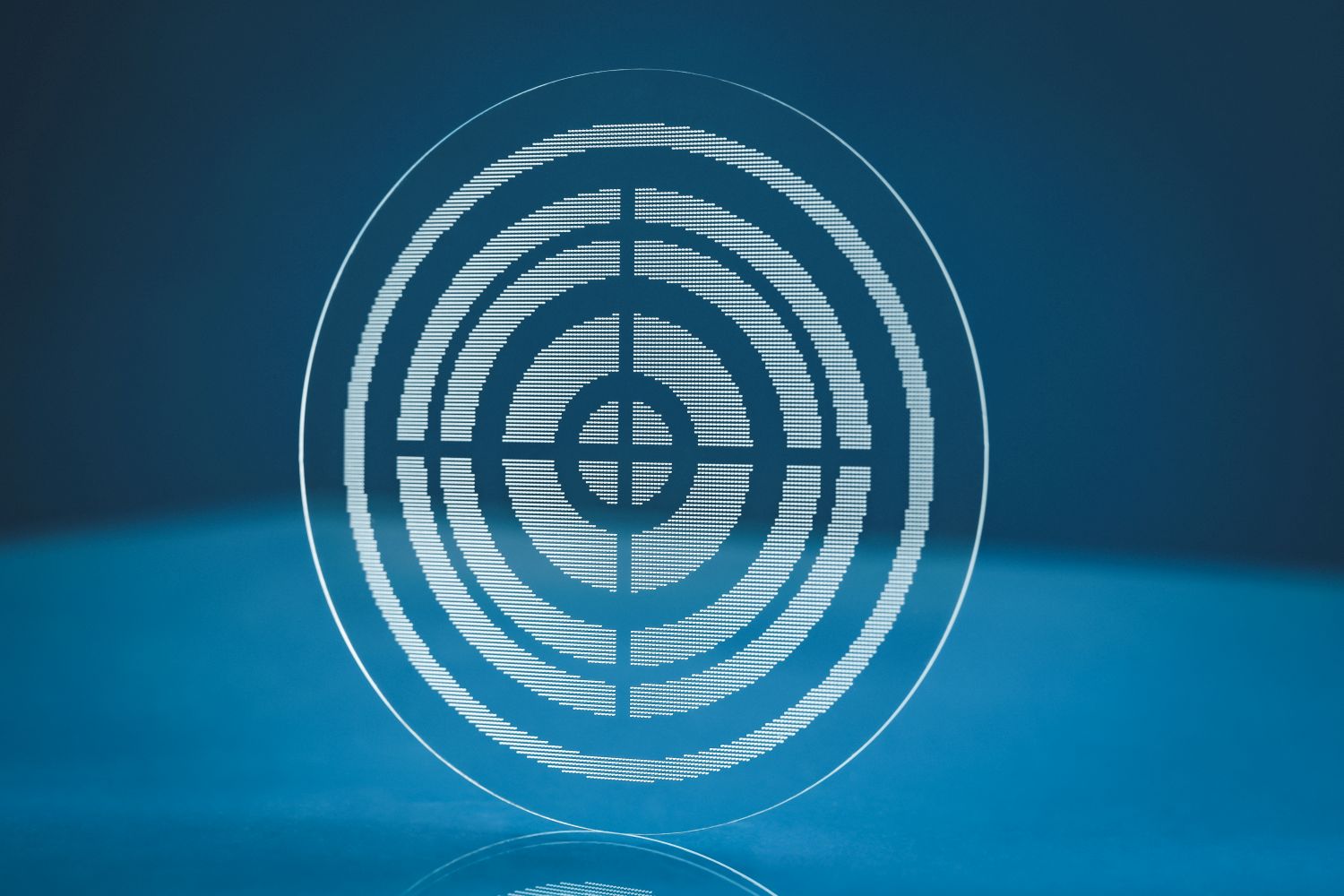
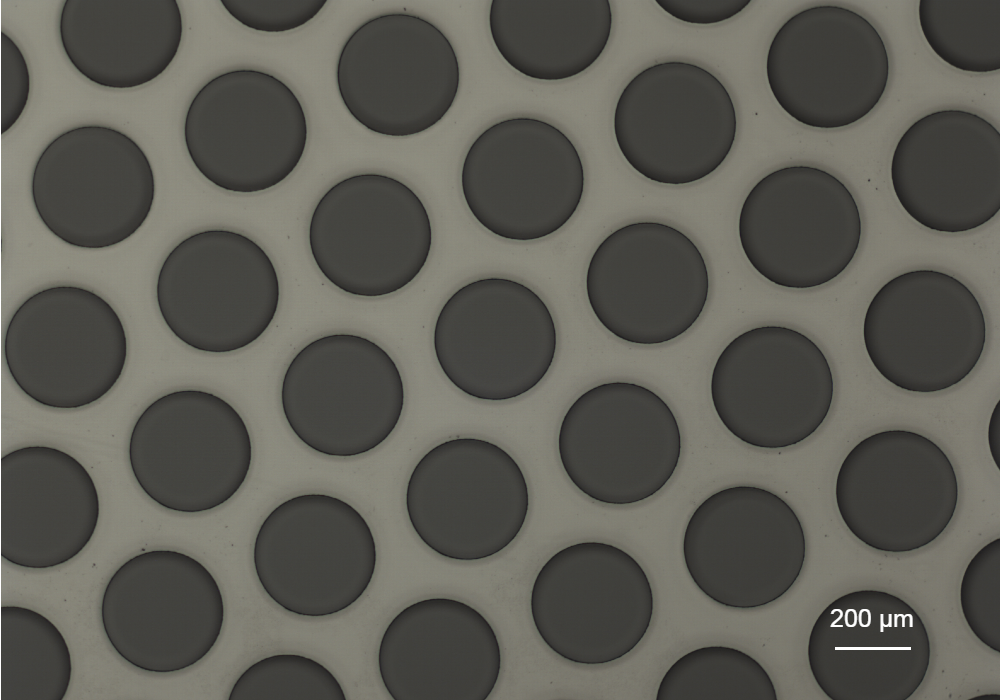
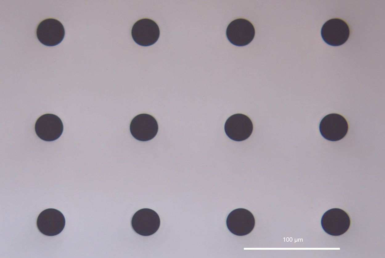
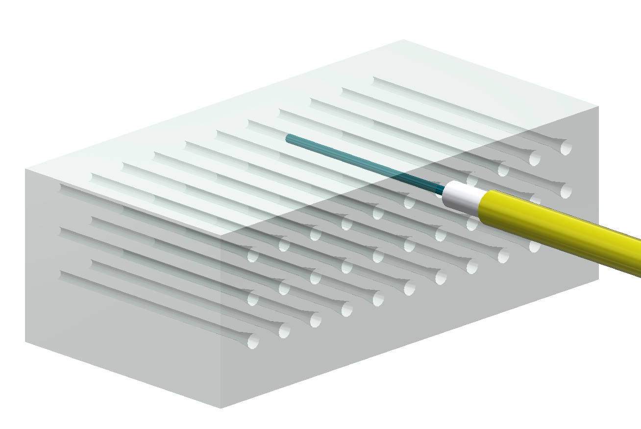
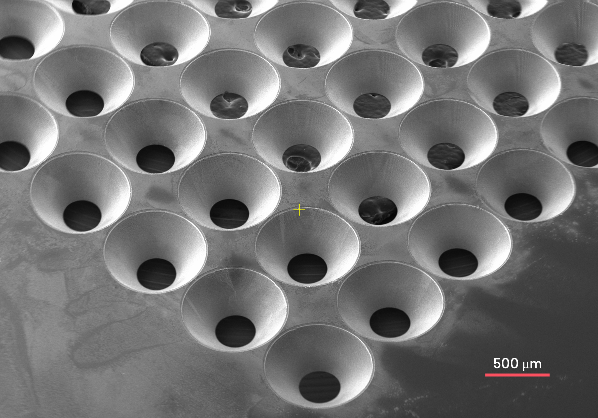
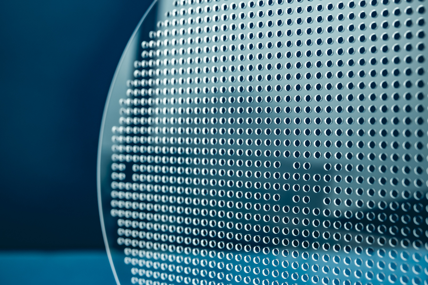
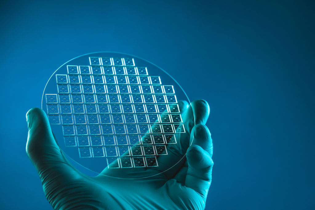
While working with glass wafer drilling, various mesh glass wafers and wafers for Wafer-level-packaging (WLP) can combine different shapes of through-holes with high aspect ratio channels in the same wafer.
We deliver high-surface quality glass wafers drilling with densely packed features that require no or minimum post-processing before being used in your production process.
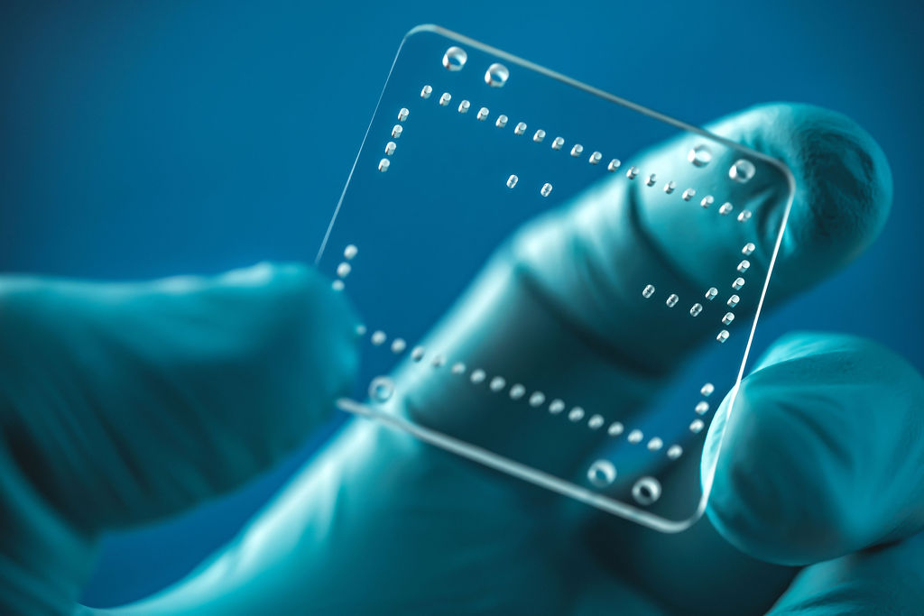
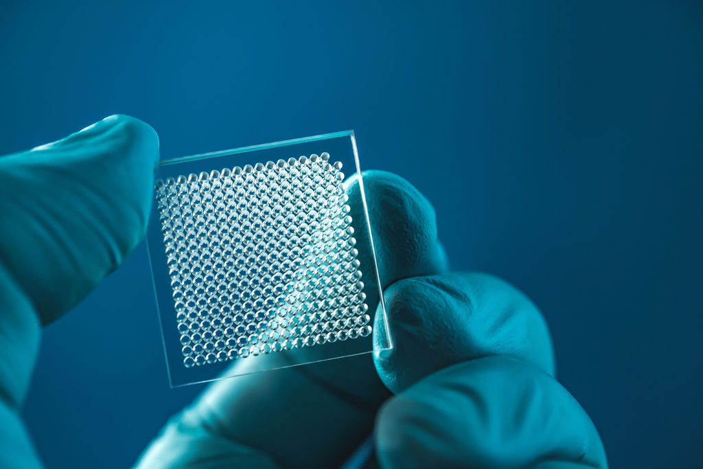
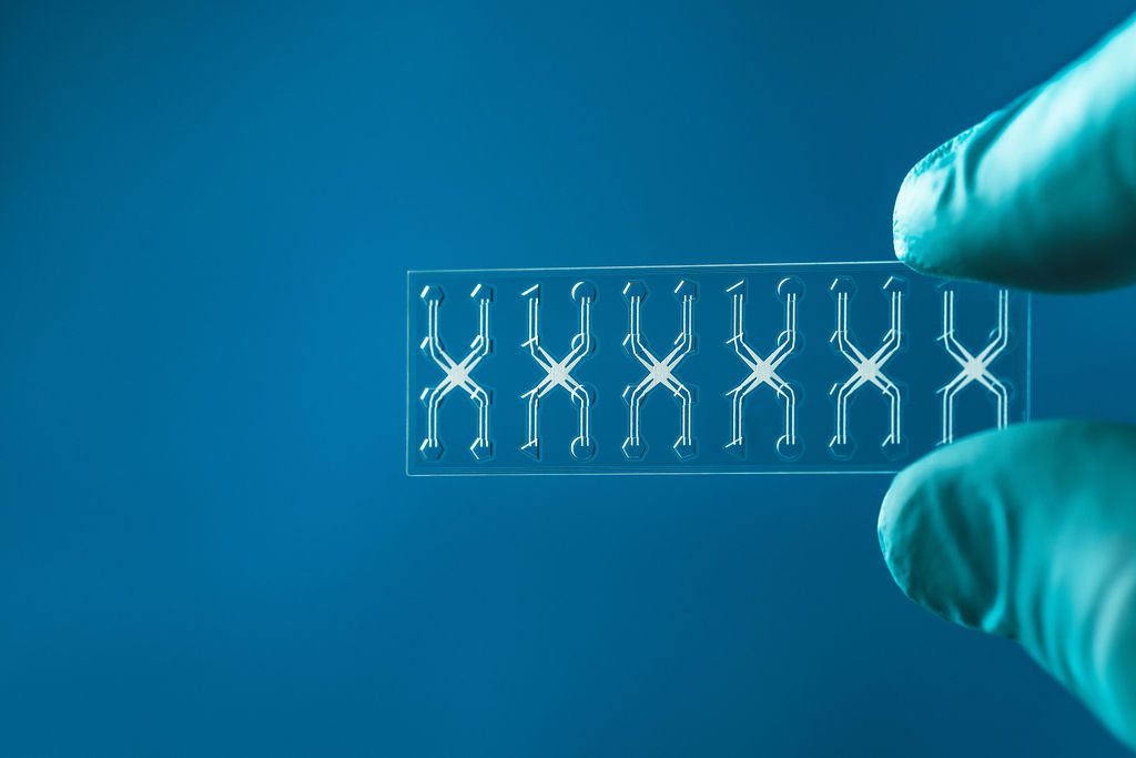
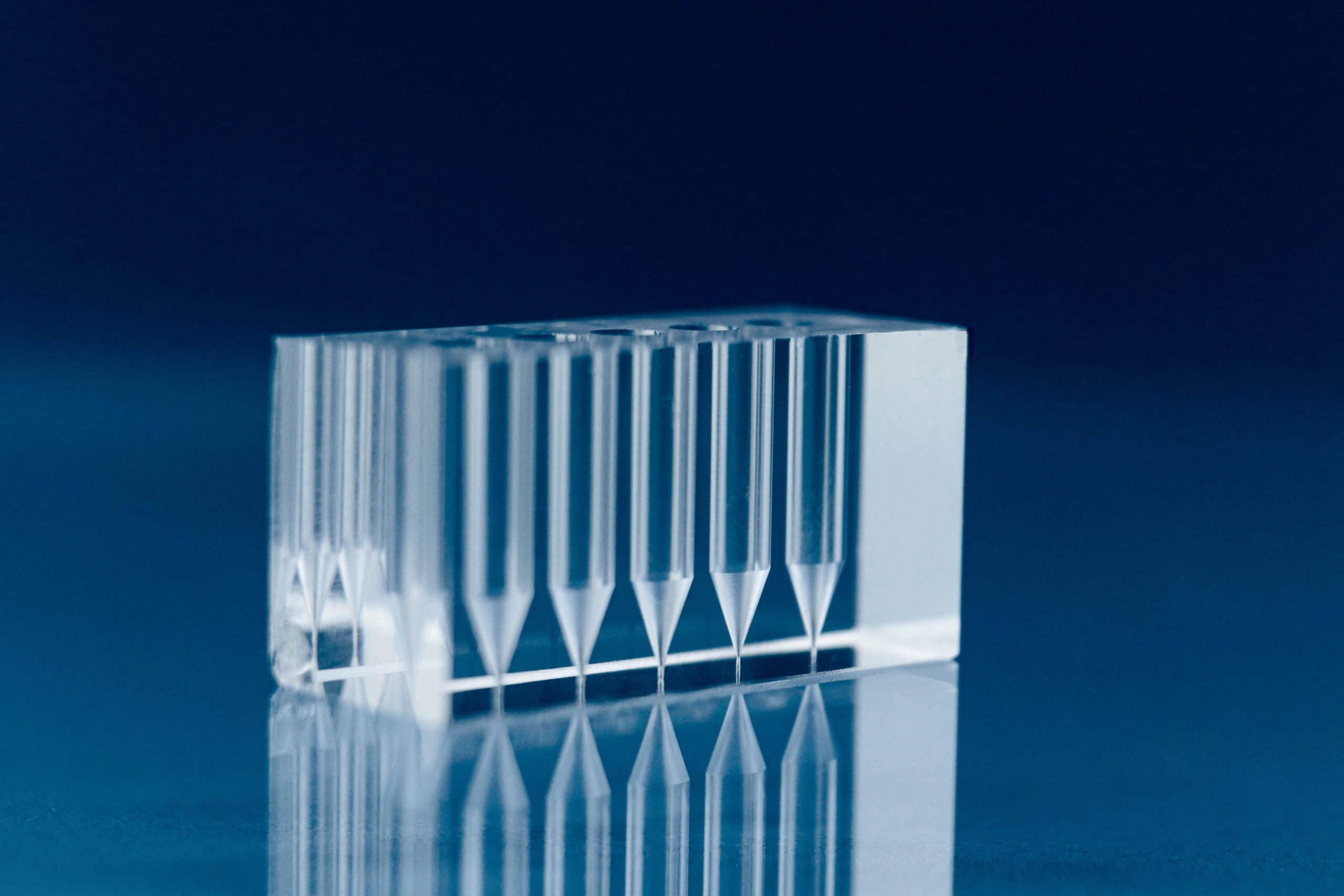
Besides glass wafer drilling, we provide a wide range of glass drilling services in parts for numerous applications: microfluidic chip channel drilling, guide plates for probe cards drilling, multiwell plates drilling, fiber alignment arrays drilling, glass needles drilling, and others.
Rapid prototyping services to test your idea in an actual environment.
Ultra-high precision production services on all materials - glass, sapphire, ceramics, silicon, optical fibers, metal, plastic.
Tailor-made laser systems for industry & science. Designed for your specific applications.
Glass & sapphire cutting and dicing workstation for industry, that outperforms other glass cutting methods.
Custom design glass microfluidic chips and devices manufacturing. Ultra-high precision results.
Glass multiwell plates designed to exact cell culture application. Circular wells, square wells, hexagon wells,…
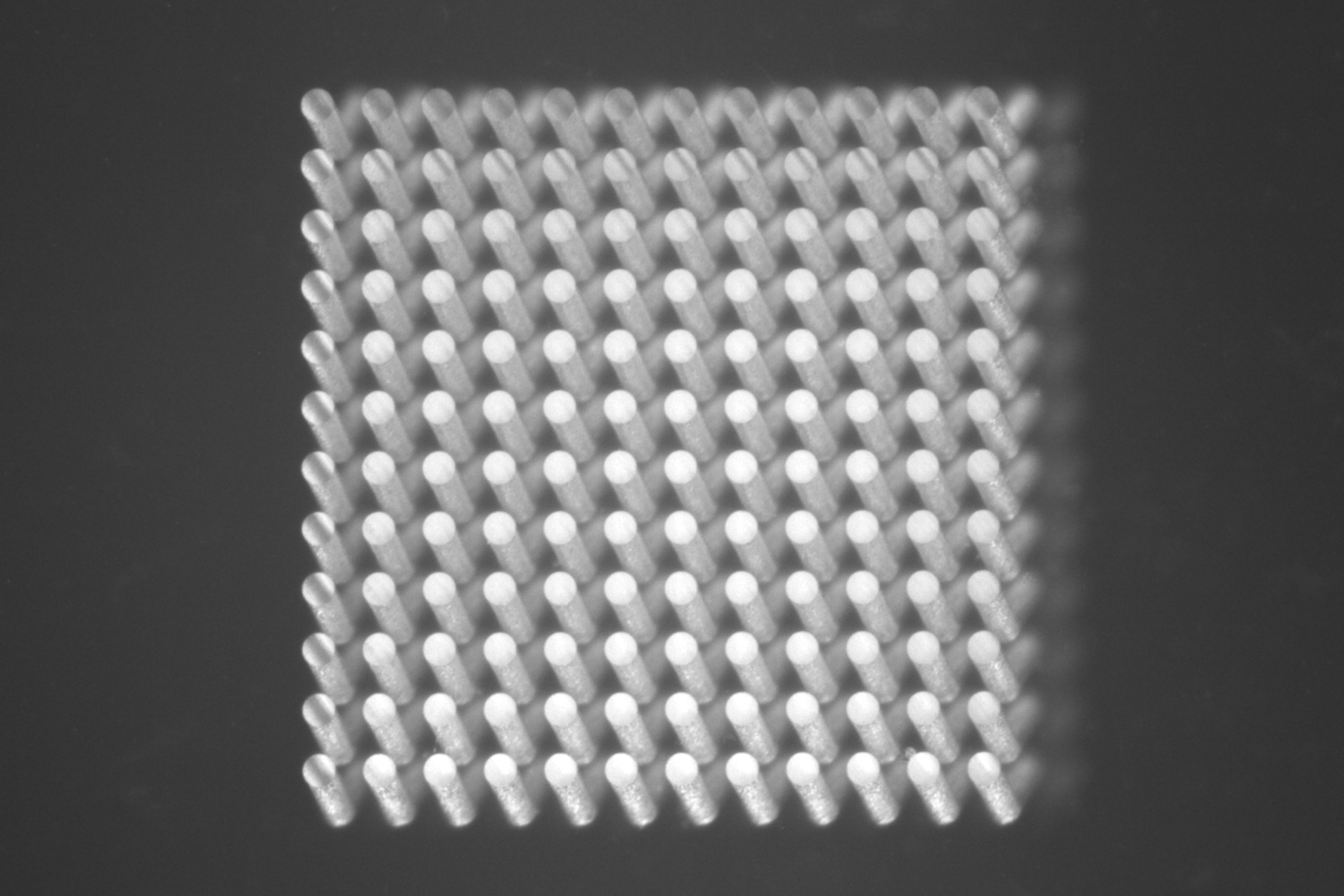
1D, 2D arrays, designed to reach ultra-precise alignment and positioning, enabling high-speed data transmission with…
WORKSHOP OF PHOTONICS
Mokslininku st. 6A, Vilnius, LT-08412, Lithuania
Phone: +370 5 215 7551
E-mail: [email protected]
Altechna R&D, UAB
Company code 301502628
VAT code LT100006155012
Bank – SEB 70440
LT87 7044 0600 0770 8092


