
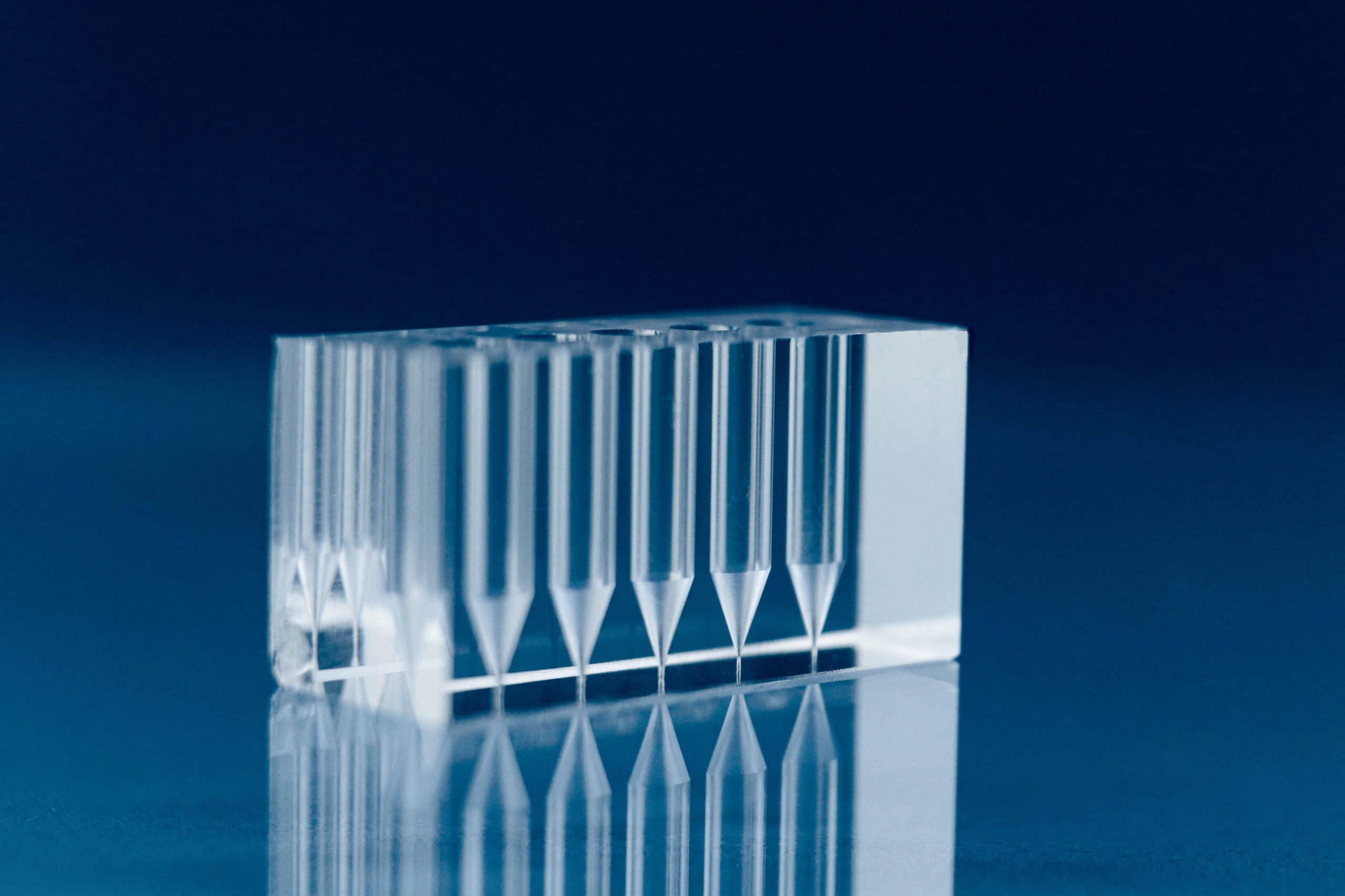
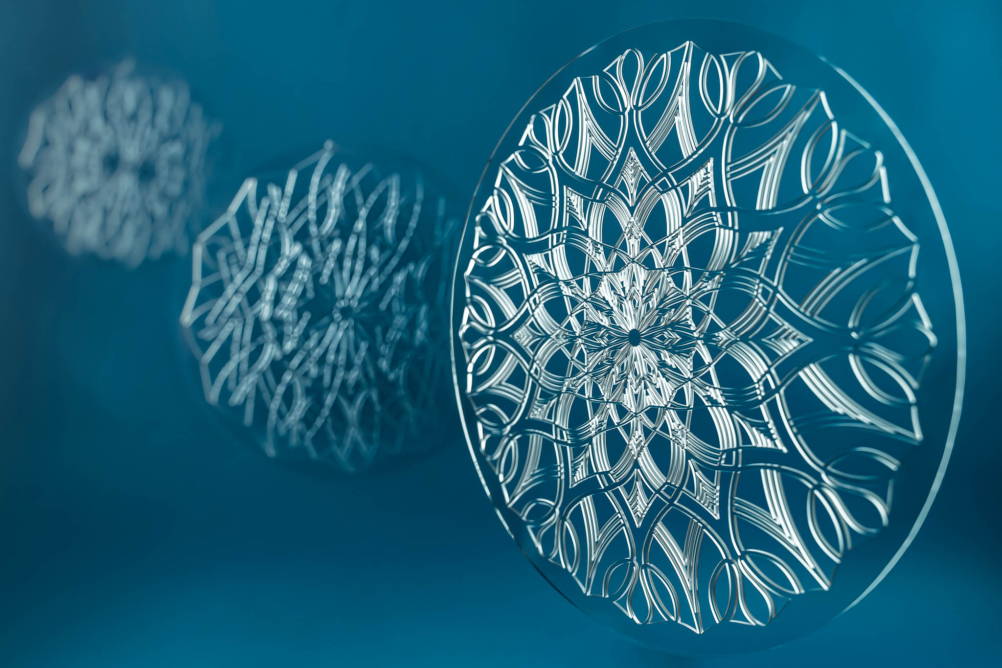
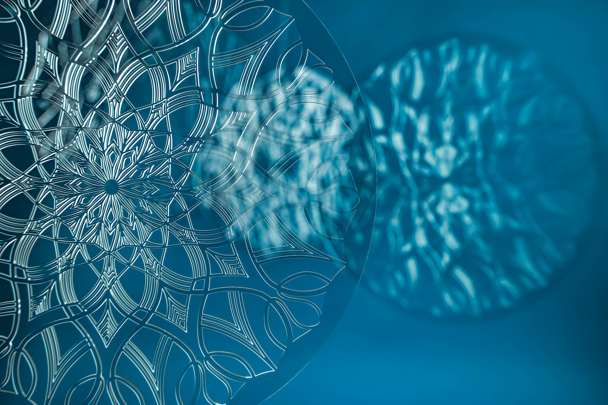
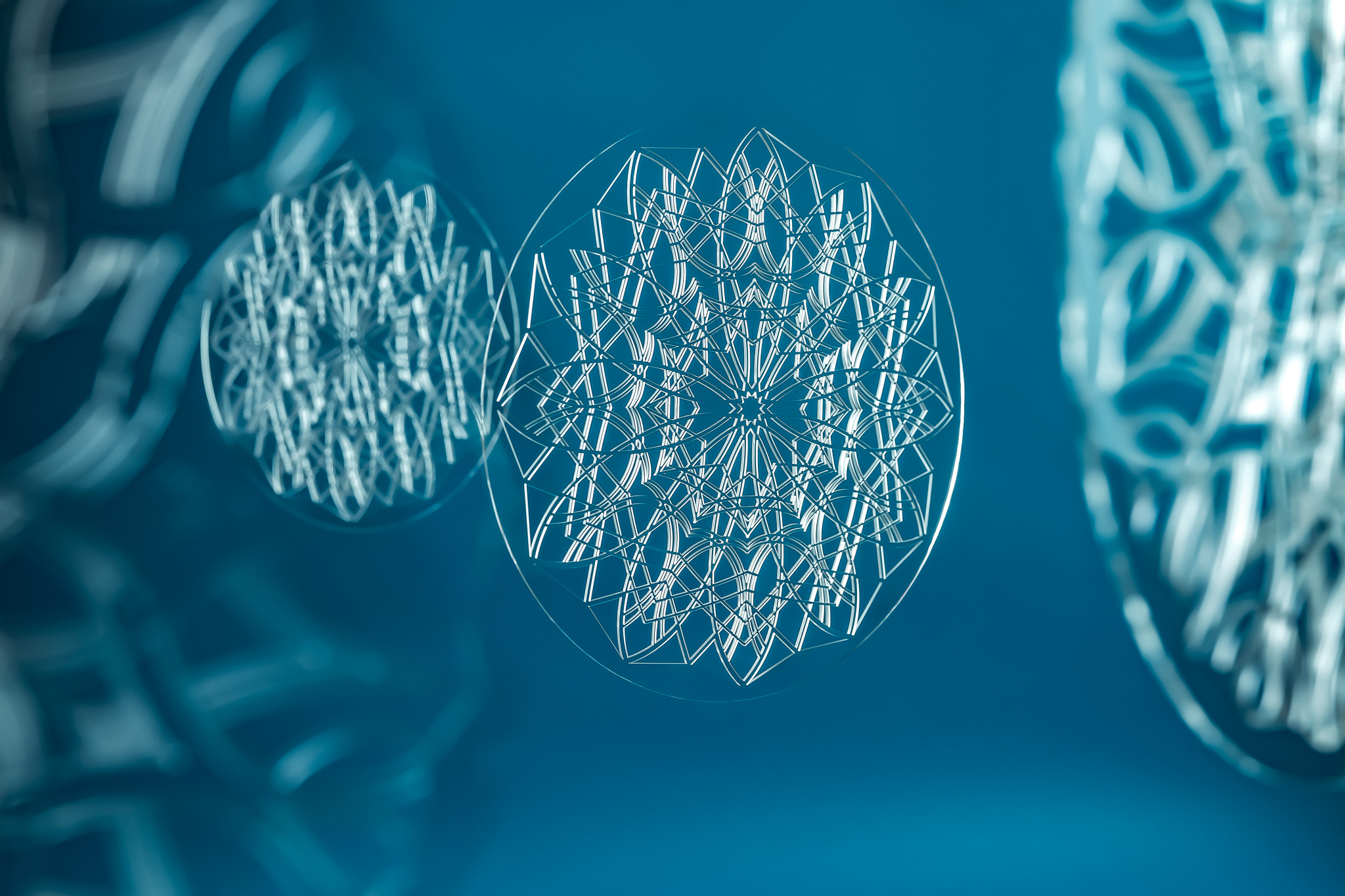
Selective laser etching for 3D glass structures
Selective laser etching (SLE) is a two-step process.
First, we modify glass by using ultra-short pulse laser radiation. Ultra-short pulses can effectively make modifications inside the transparent materials, and only one pulse is enough to go through the substrate. It ensures speed and quality for volume production.
Second, we remove the modified areas using wet chemical etching. Selective (SLE) means that modified areas are affected by etching much faster than unmodified ones, making it possible to achieve the desired result.
We have optimized the process achieving sufficient accuracy with speed suitable for the industry.
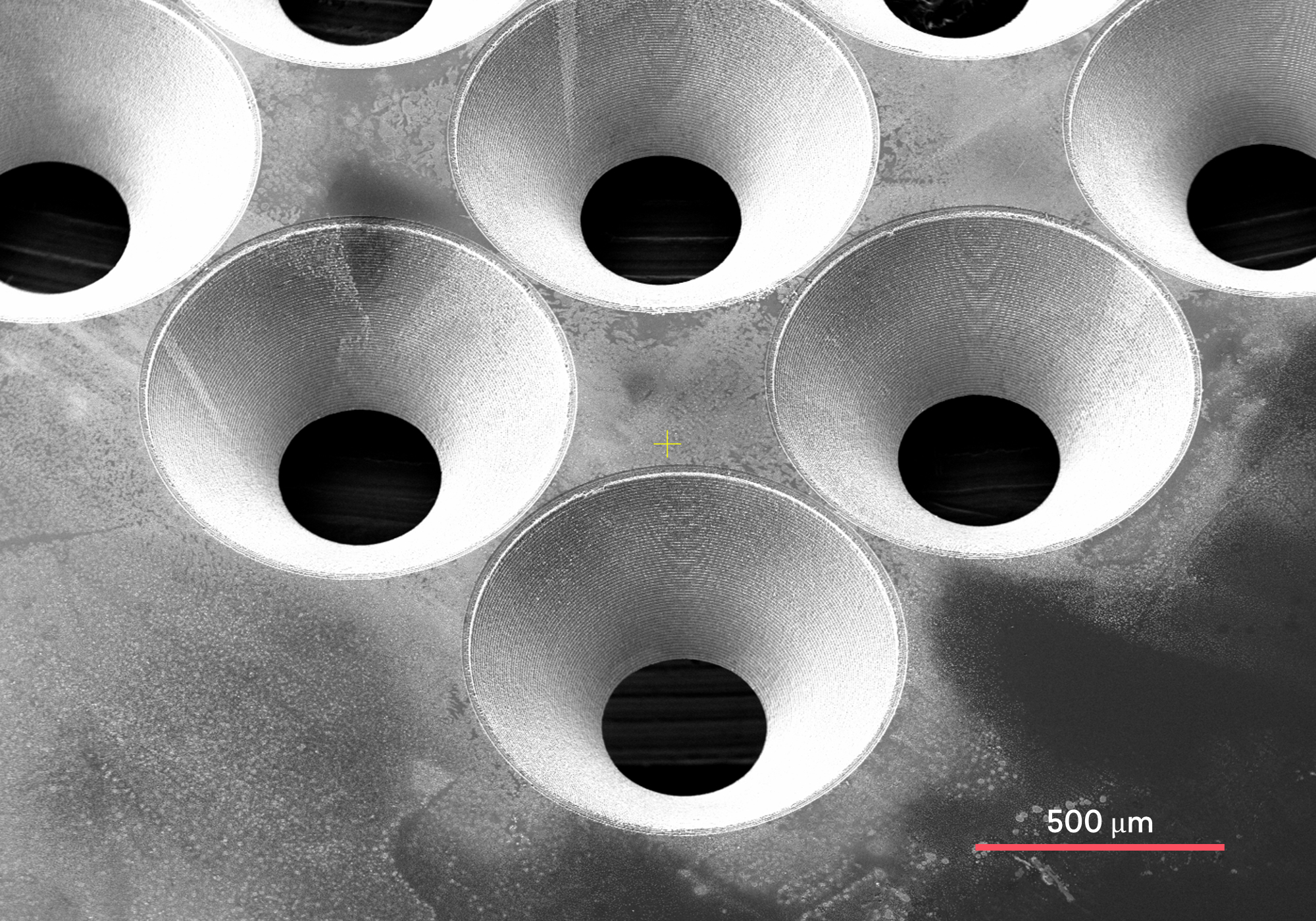
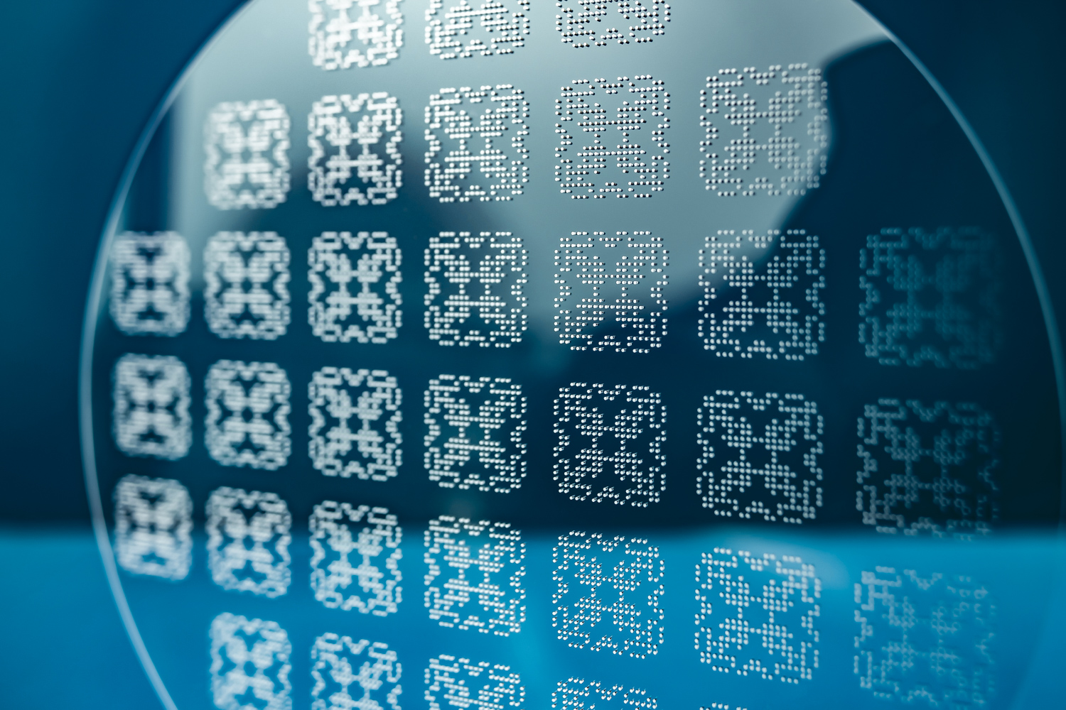
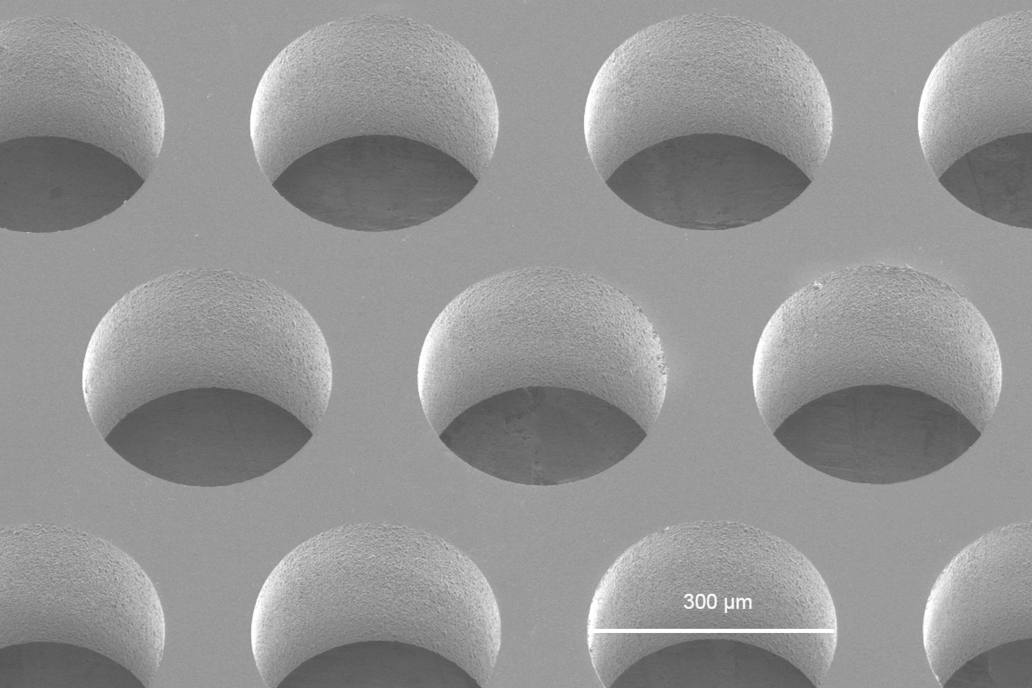
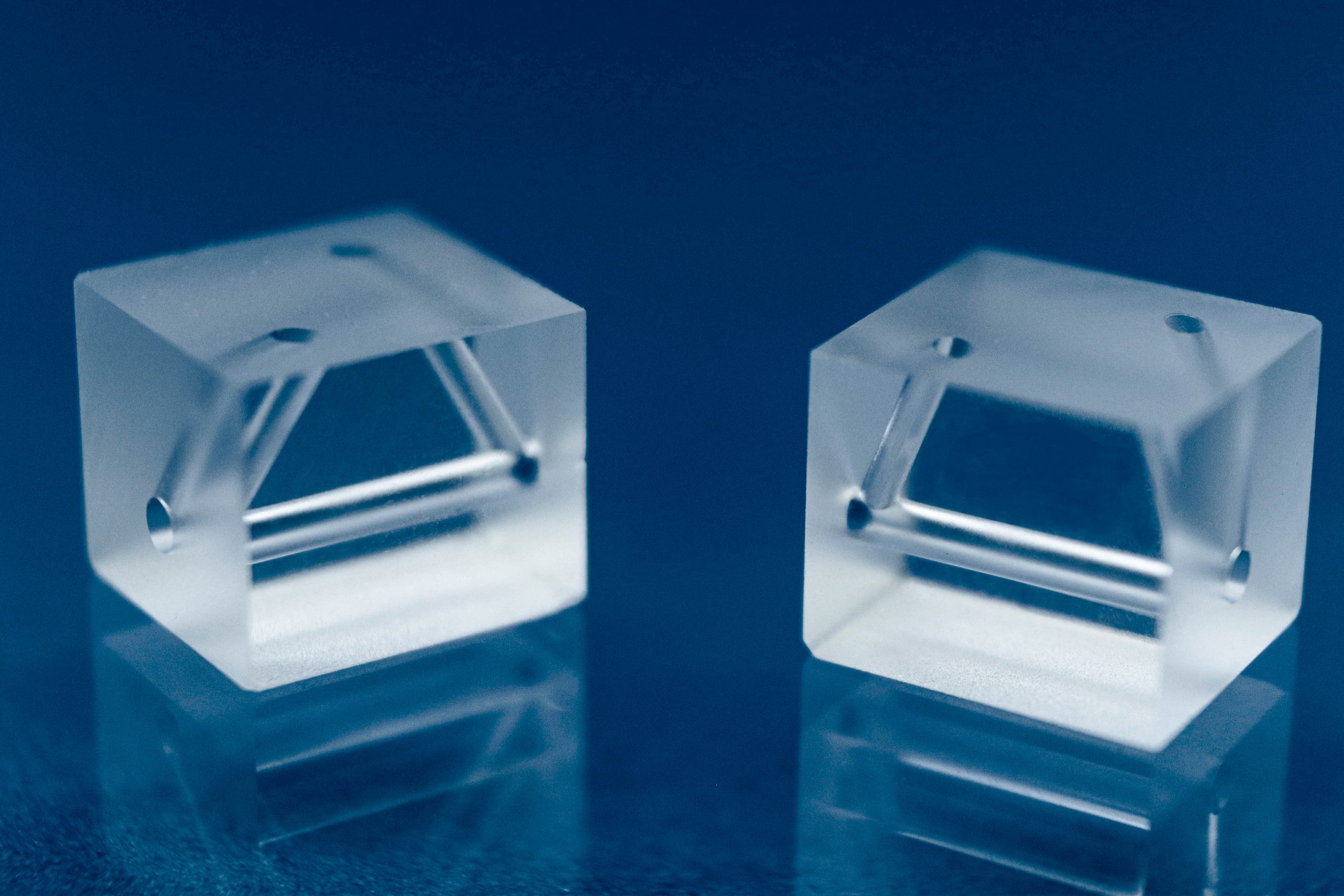
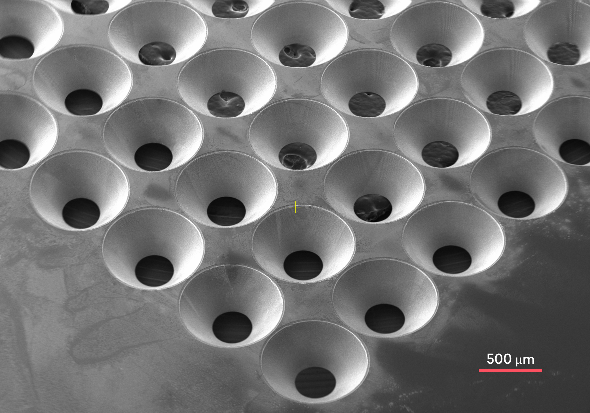
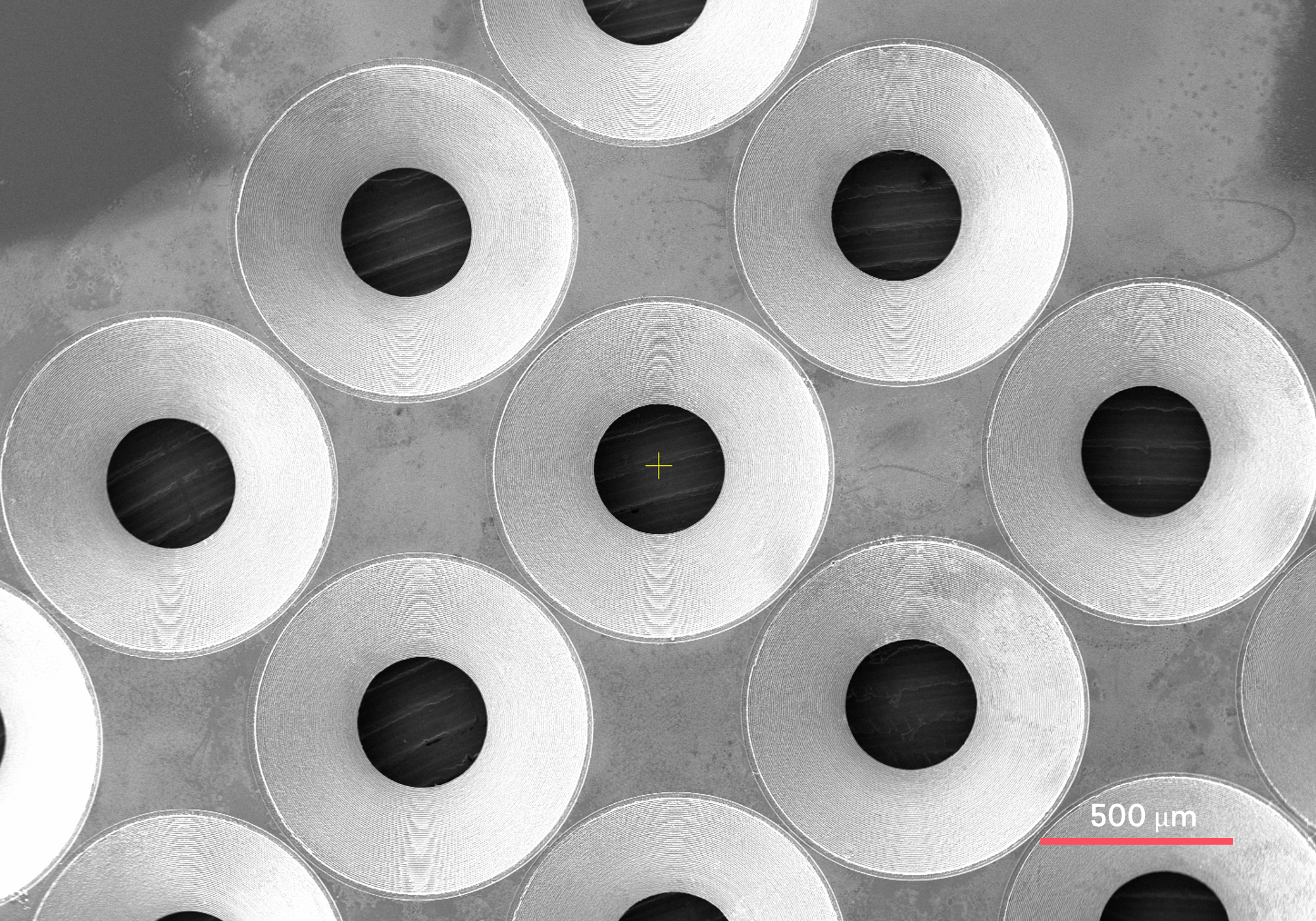
Custom design glass microfluidic chips and devices manufacturing. Ultra-high precision results.
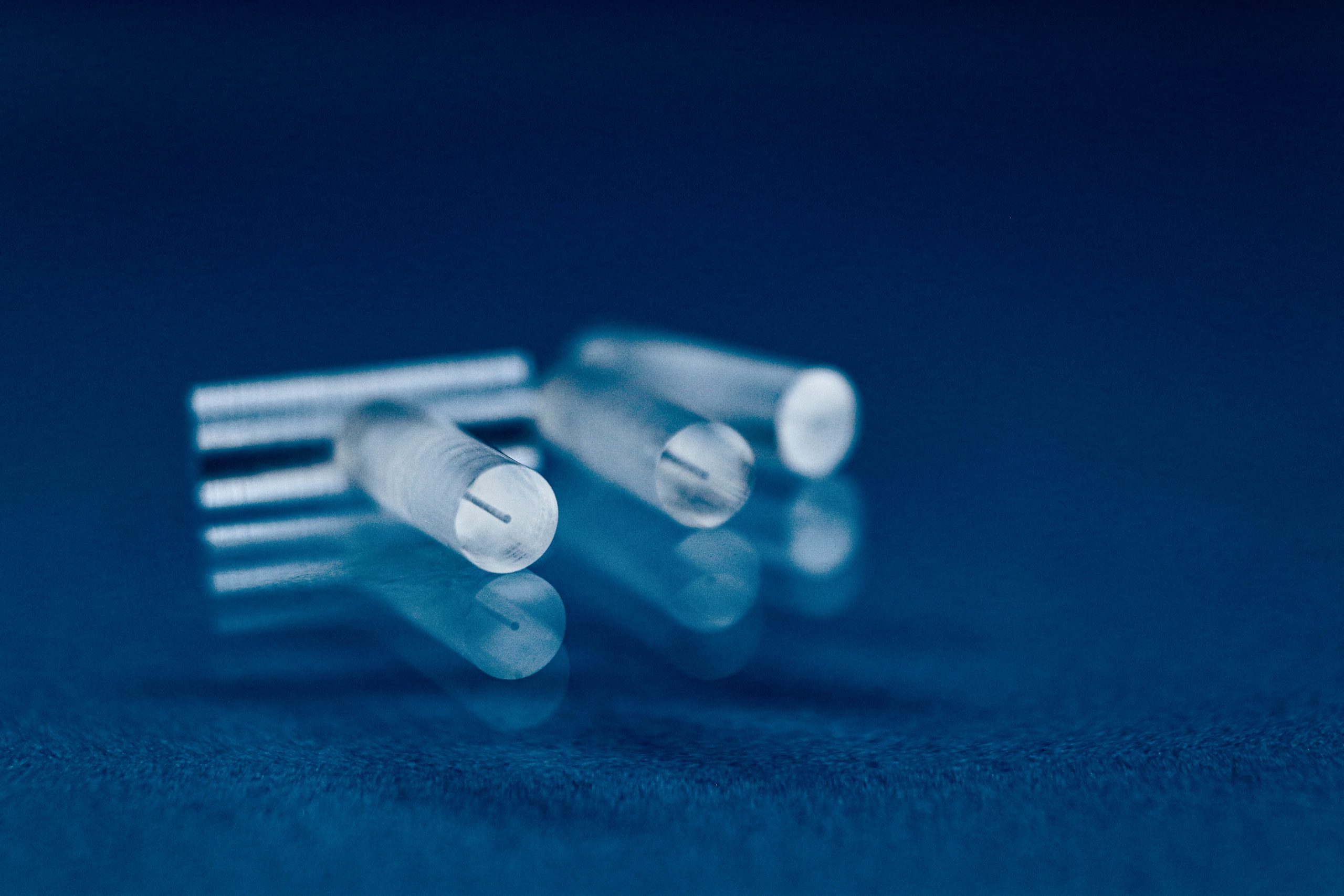
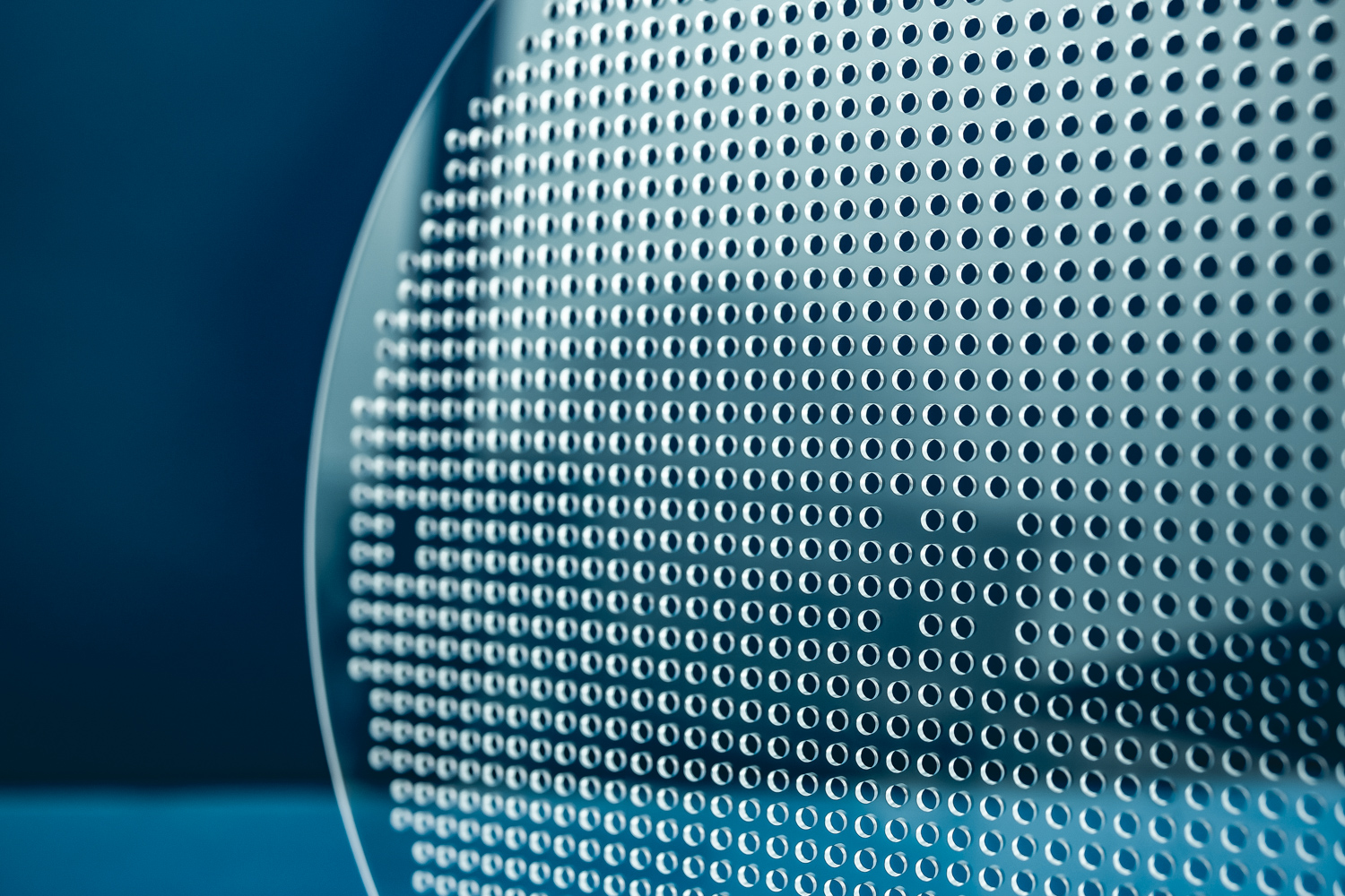
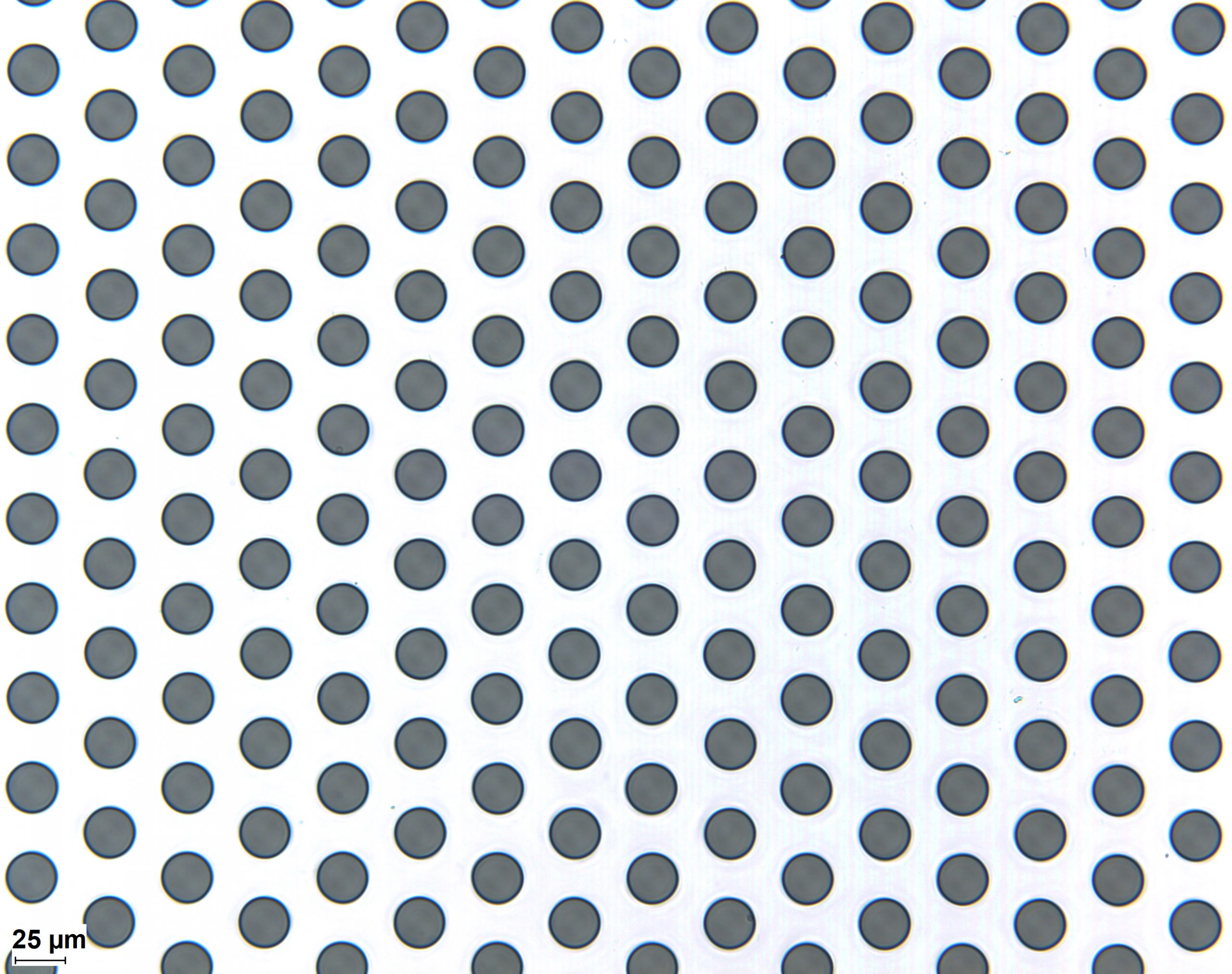
We offer ultra-high precision laser glass micro drilling. Highest quality in the market.
Suitable for 2.5D / 3D integration and wafer-level bonding with semiconductor substrates for MEMS, sensors,…
Ceramic plates and glass plates for the probe cards industry – an essential component for…
Rapid prototyping services to test your idea in an actual environment.
Ultra-high precision production services on all materials - glass, sapphire, ceramics, silicon, optical fibers, metal, plastic.
Tailor-made laser systems for industry & science. Designed for your specific applications.
WORKSHOP OF PHOTONICS
Mokslininku st. 6A, Vilnius, LT-08412, Lithuania
Phone: +370 5 215 7551
E-mail: [email protected]
Altechna R&D, UAB
Company code 301502628
VAT code LT100006155012
Bank – SEB 70440
LT87 7044 0600 0770 8092


