


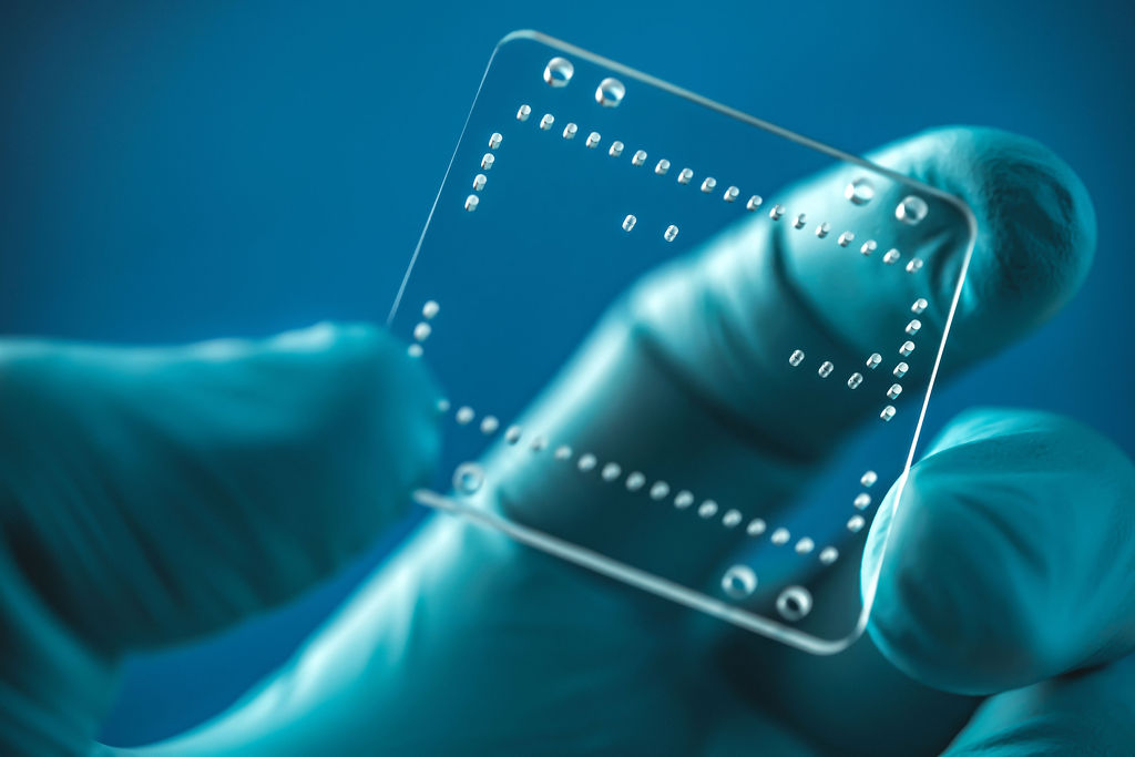
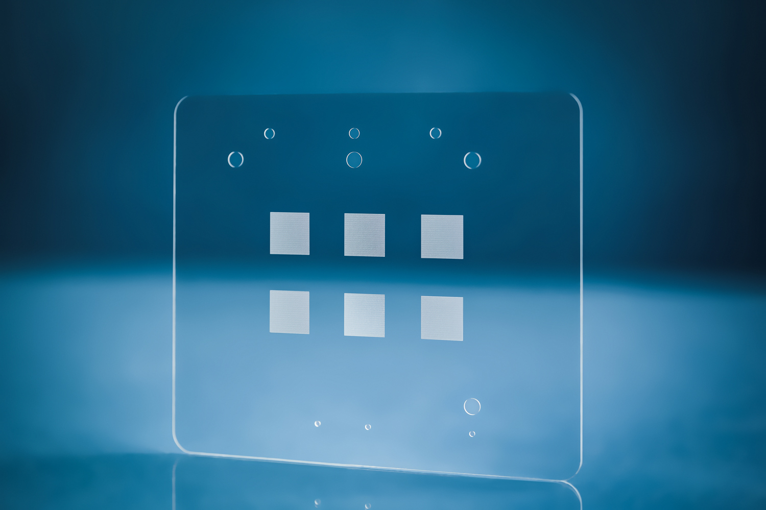
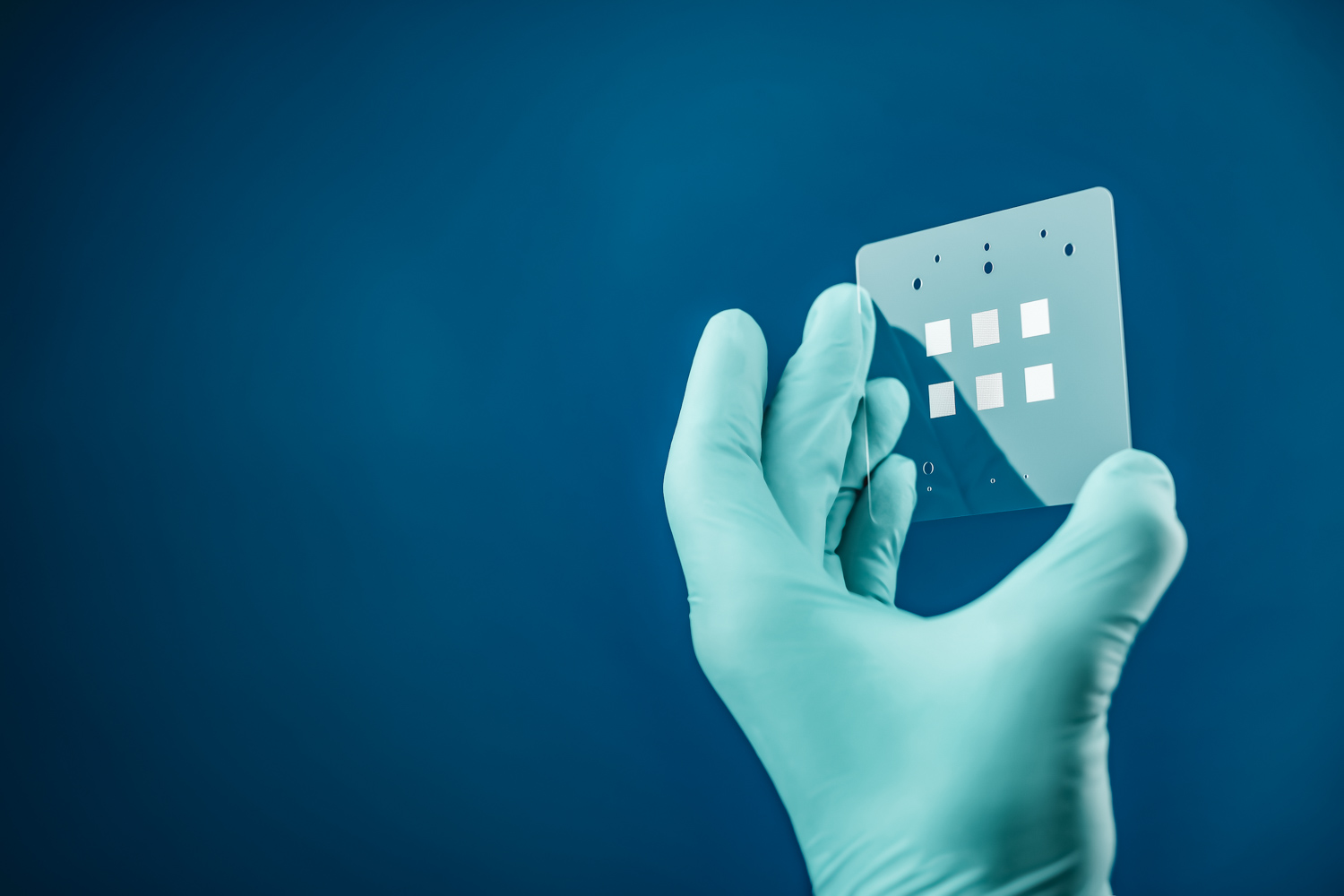
While we achieve outstanding results with both – glass and ceramics, we suggest thinking of using GLASS for your guide plates.
Rapid prototyping services to test your idea in an actual environment.
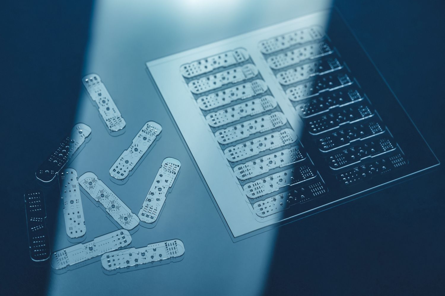
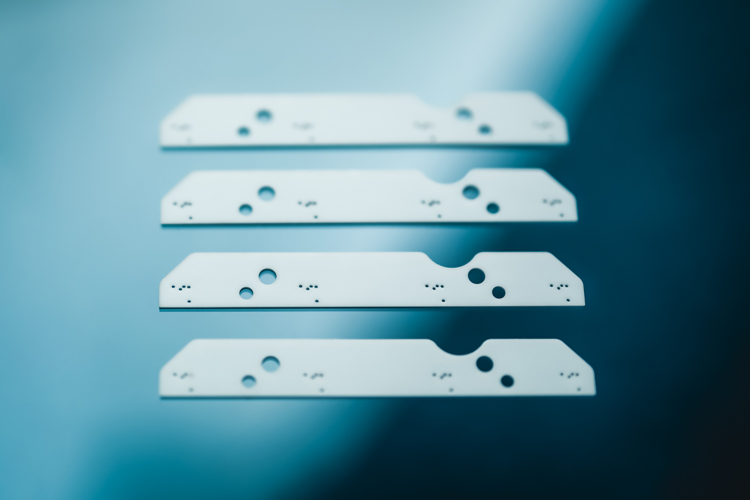
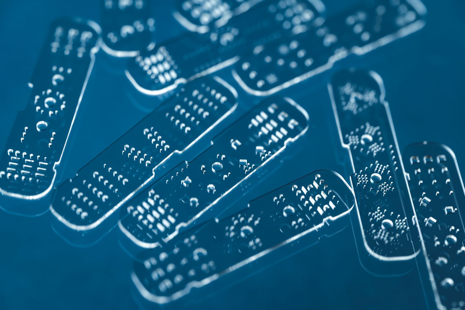
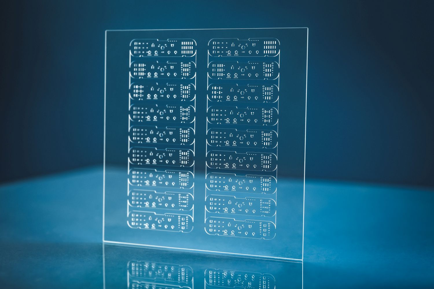
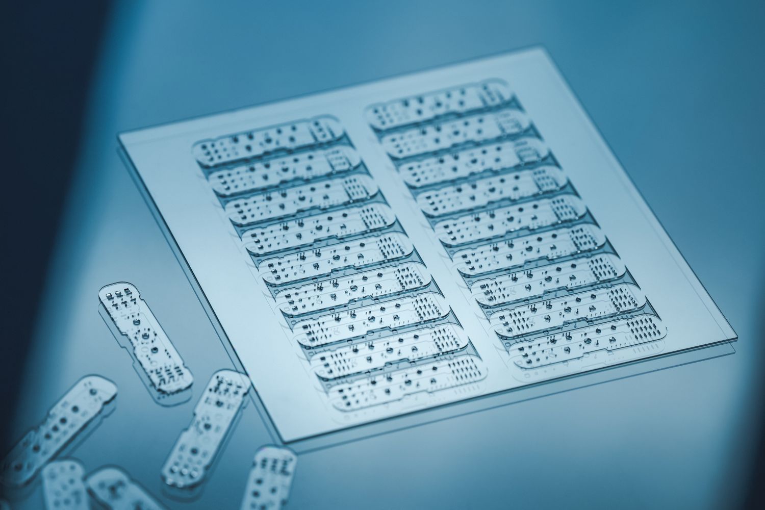
Ultra-high precision production services on all materials - glass, sapphire, ceramics, silicon, optical fibers, metal, plastic.
Tailor-made laser systems for industry & science. Designed for your specific applications.
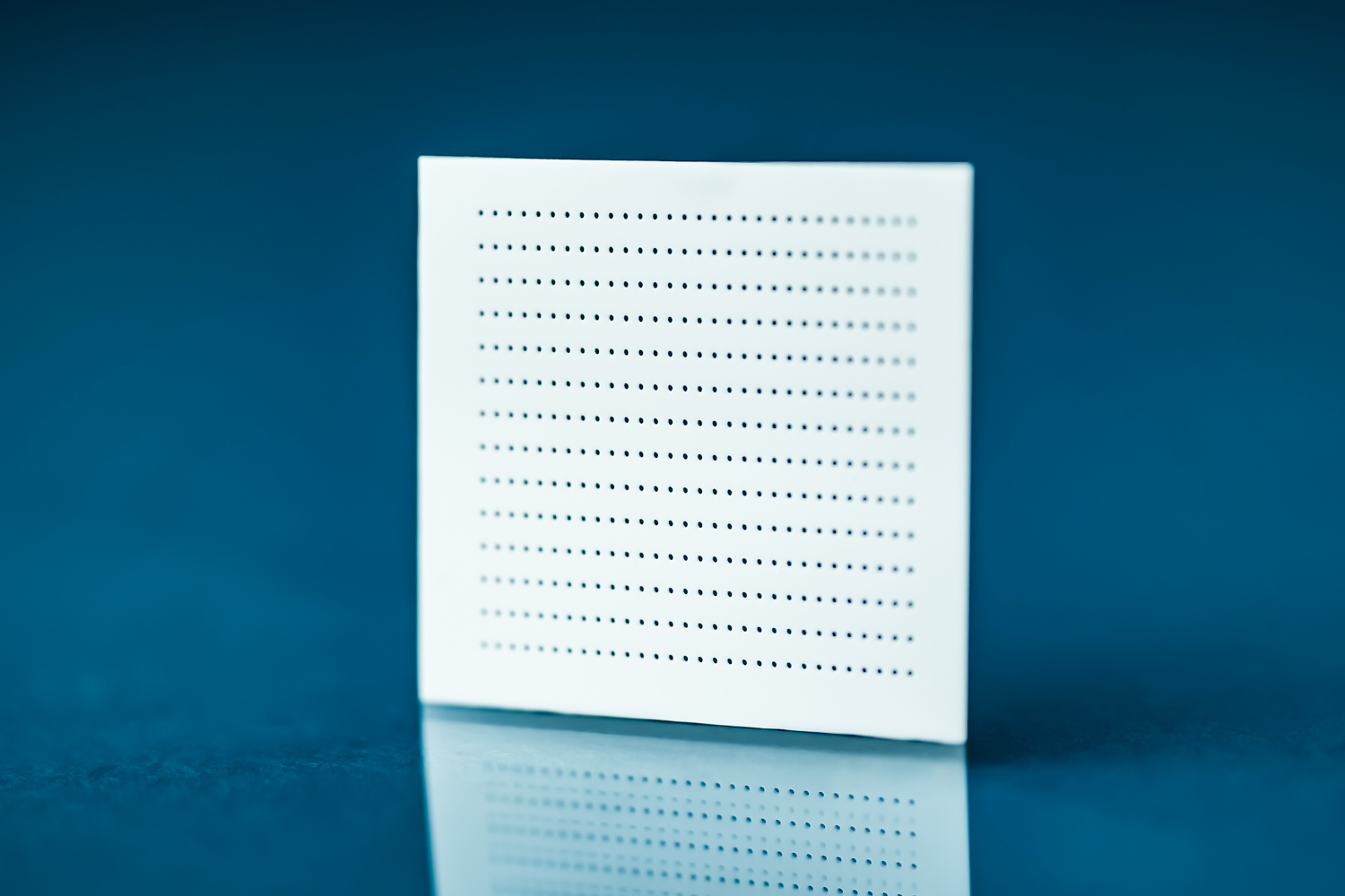
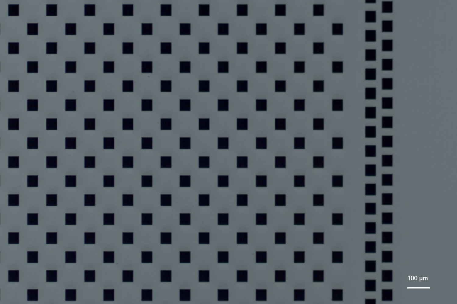
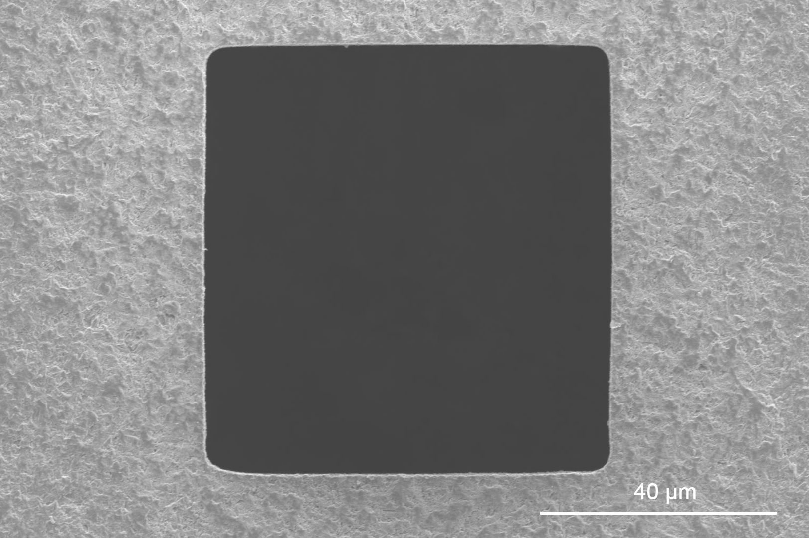
We offer ultra-high precision laser glass micro drilling. Highest quality in the market.
High processing speed Ultra-high accuracy Minimal heat-affected zone Various shapes holes No melting or micro-cracks…
High processing speed Ultra-high accuracy Minimal heat-affected zone Various shapes holes No melting or micro-cracks…
Glass & sapphire cutting and dicing workstation for industry, that outperforms other glass cutting methods.
WORKSHOP OF PHOTONICS
Mokslininku st. 6A, Vilnius, LT-08412, Lithuania
Phone: +370 5 215 7551
E-mail: [email protected]
Altechna R&D, UAB
Company code 301502628
VAT code LT100006155012
Bank – SEB 70440
LT87 7044 0600 0770 8092


