Fiber Alignment Arrays Fabrication

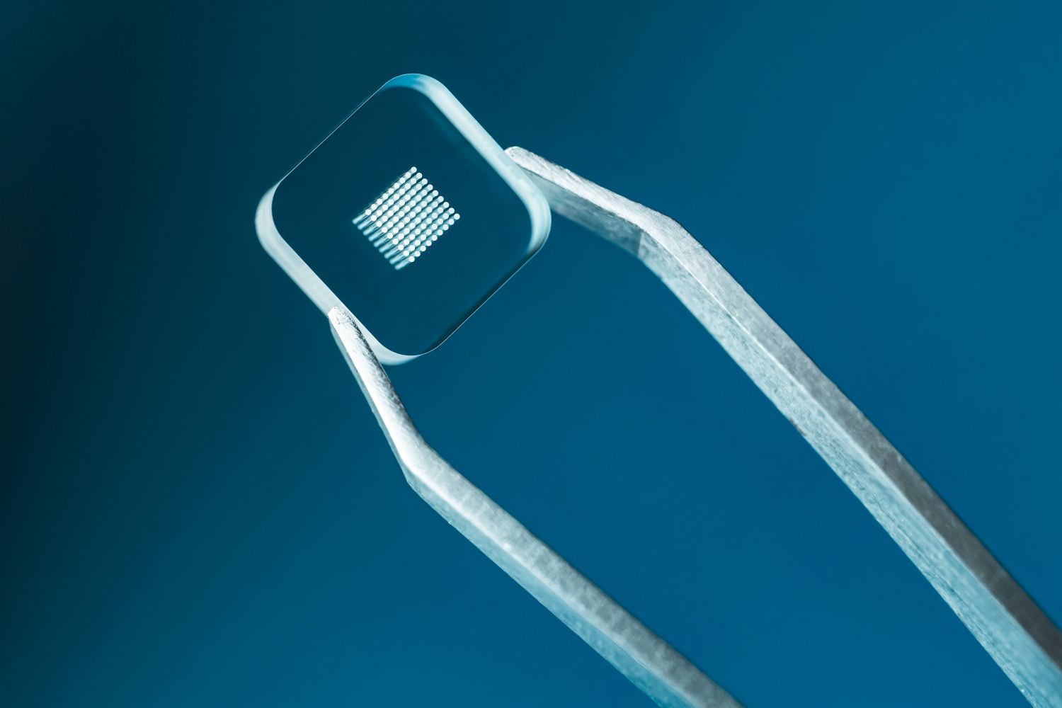
We offer optical fiber alignment arrays (1D, 2D micro-hole arrays) fabrication services.

Our solution enables reaching excellent precision results in optical fiber alignment array fabrication – the crucial component in optical communication systems – resulting in low-loss, high-speed, large-capacity communication.

Laser micromachining, together with the selective laser induces etching SLE which we use for fiber alignment structures production, offers definite advantages in terms of precision, consistency, speed, material versatility, and cost-effectiveness.

Features:

  • Ultra-high precision
  • Tight tolerances within ±0.5 µm
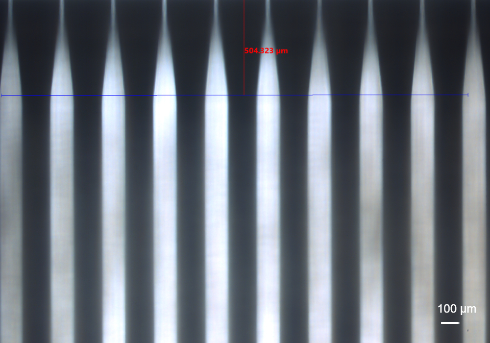
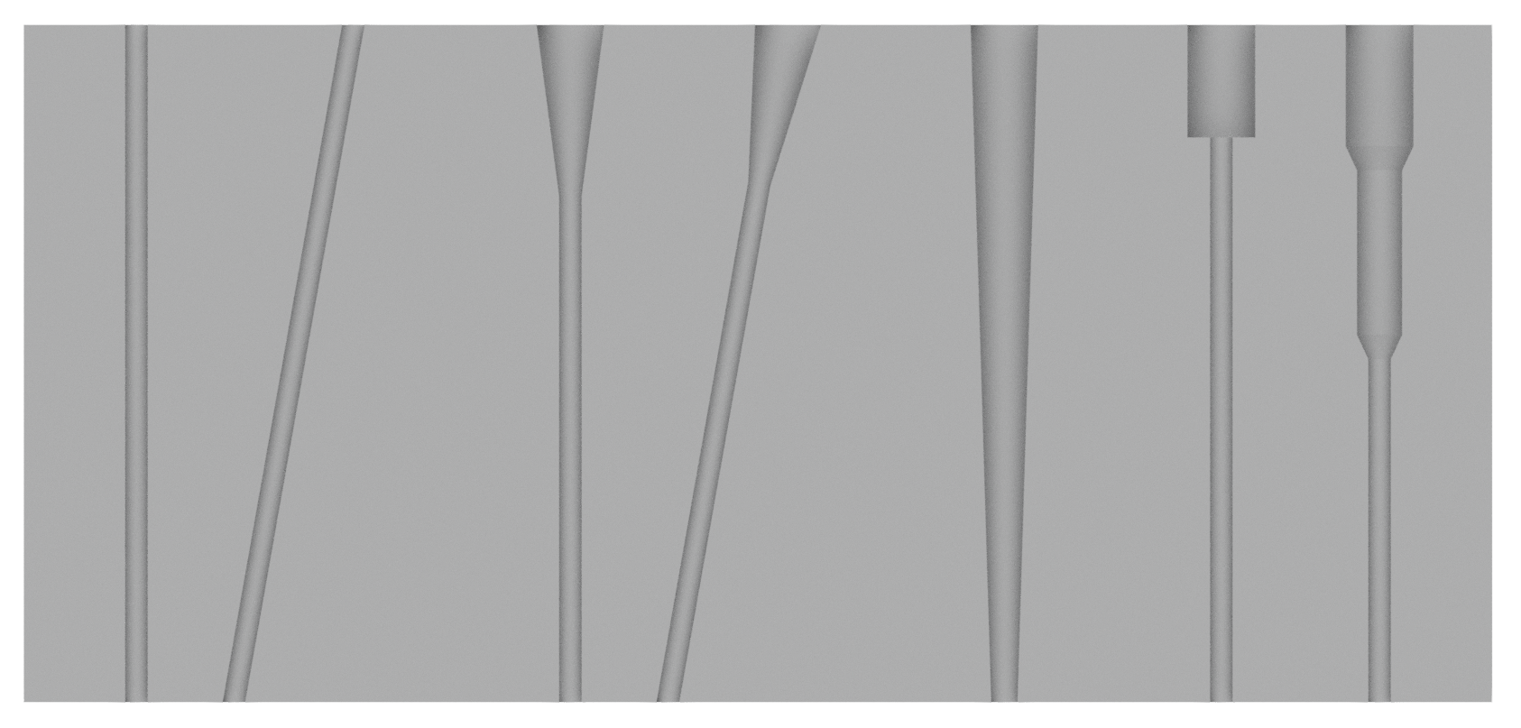
  • Straight, flared, or with a cone for easier insertion
  • Designed for standard SMF fibers, diameter 125/250 µm, also reduced clad fiber 80 µm (not limited)
  • High density, standard 0,25 mm pitch
  • Straight or angled holes

Fiber Arrays technical specifications

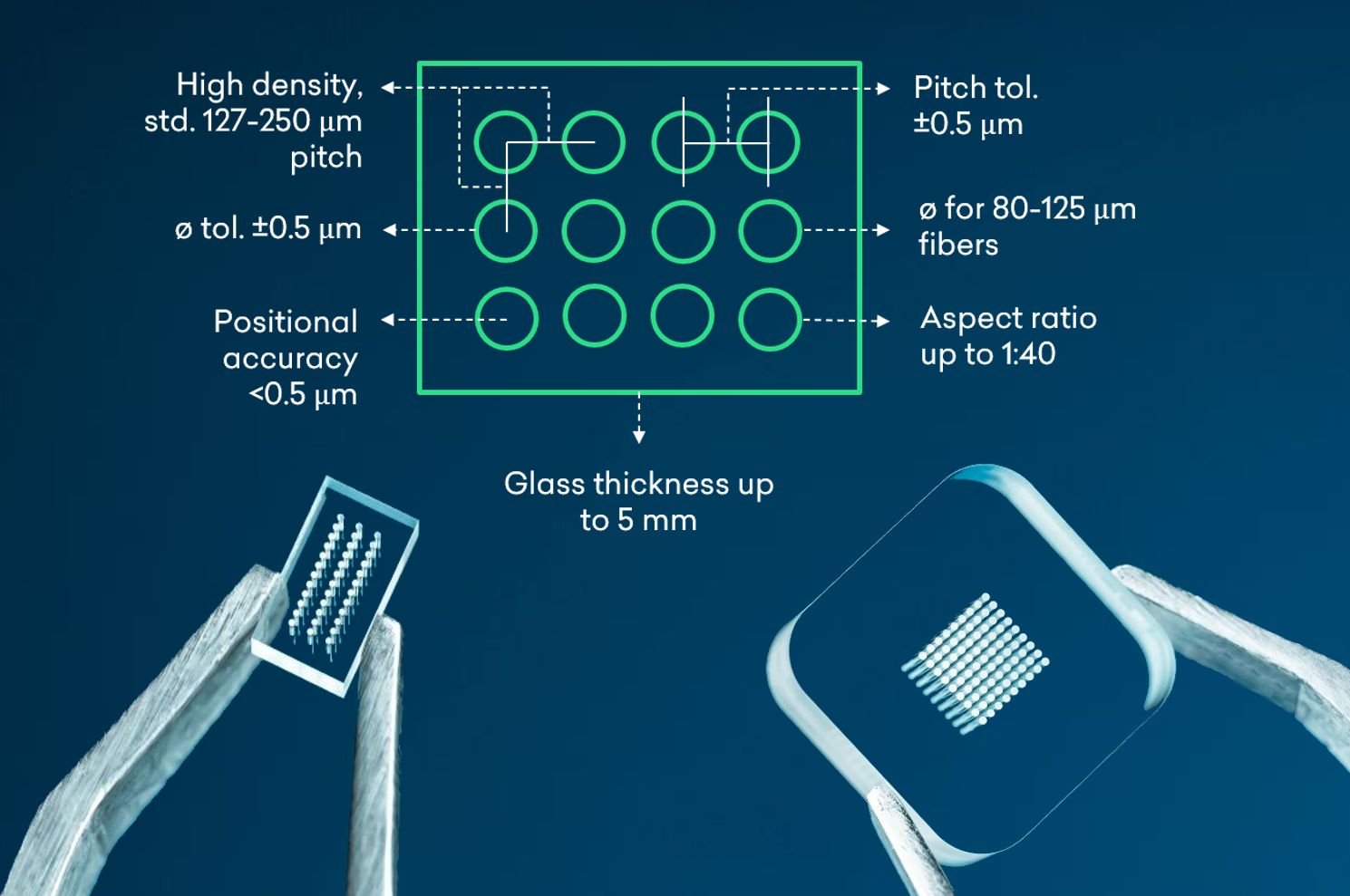
Fiber Arrays Main Features Scheme

  • Designed for standard SMF fibers, diameter 125/250 µm, also reduced clad fiber 80 µm (not limited to it)
  • High density, standard 0,25 mm pitch
  • Circularity < 1 µm diameter
  • Diameter tolerance ± 0,5 µm
  • Pitch tolerance ± 0,5 µm
  • Positional accuracy < 0,5 µm
  • Straight, flared, or with a cone for easier insertion
  • Straight or angled holes

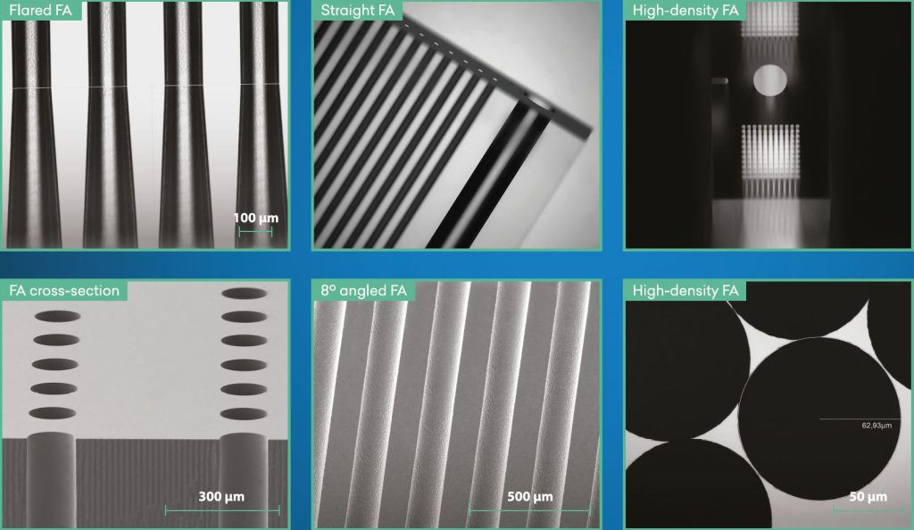
Fiber Arrays examples

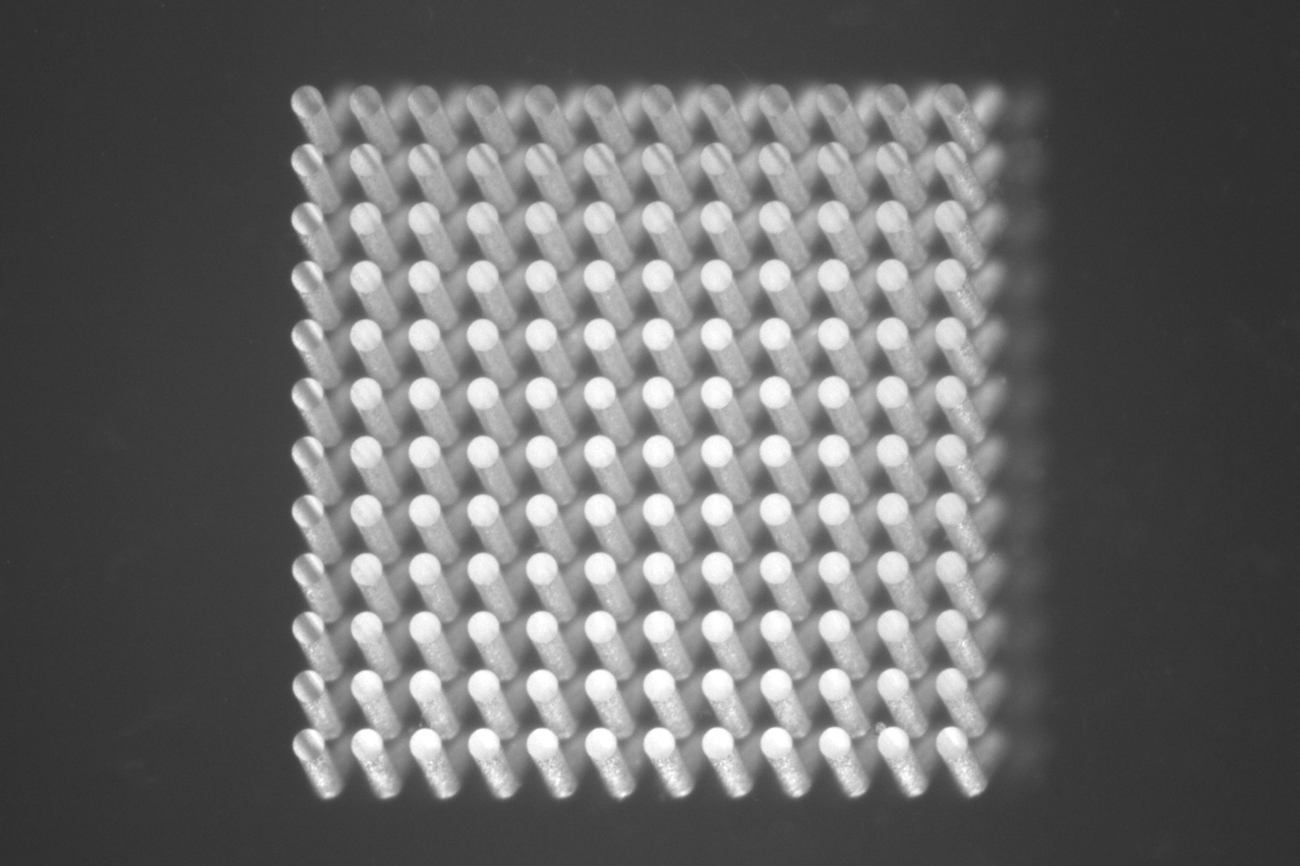
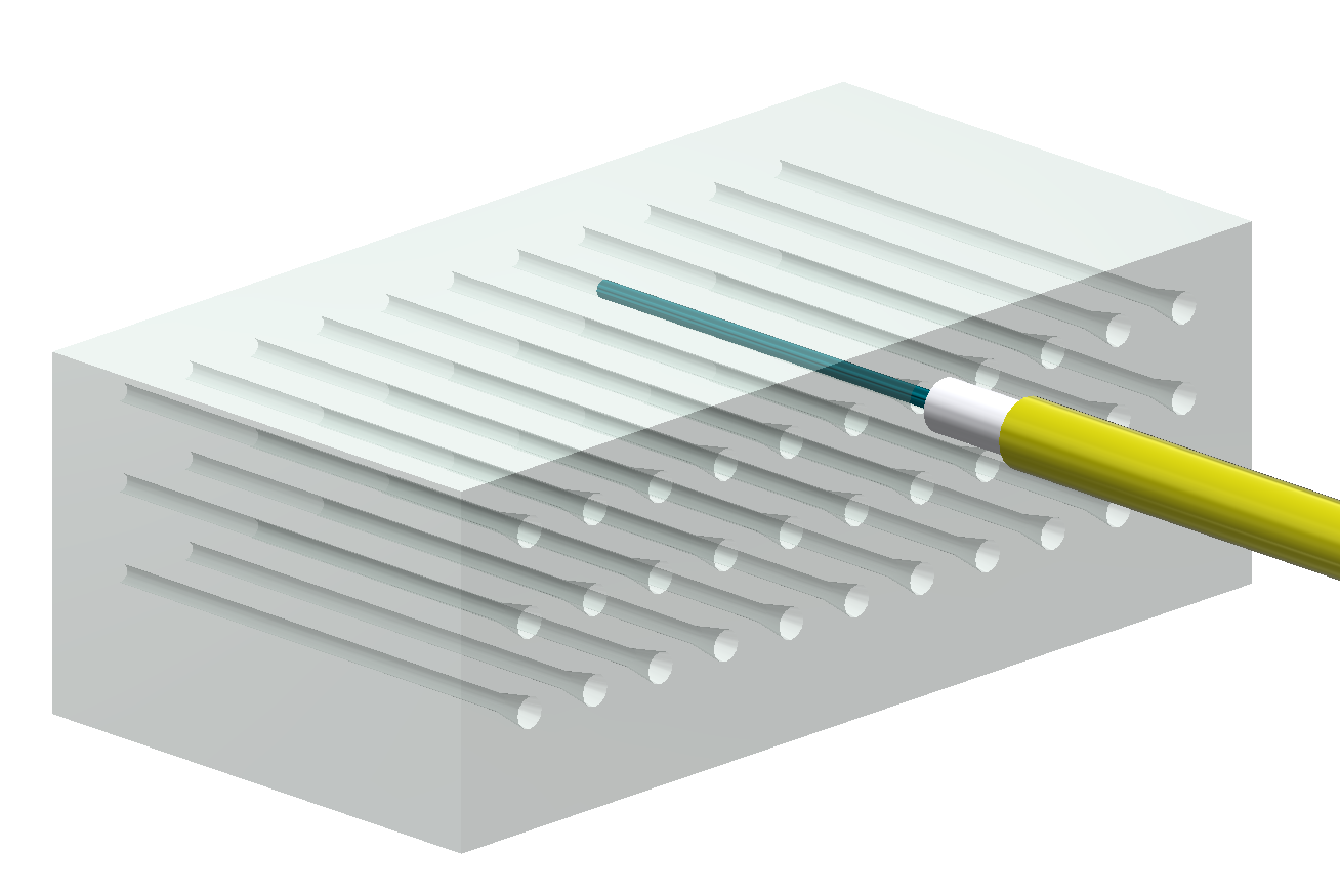
While there are one-dimensional (1D) and two-dimensional (2D) arrays, the need for speed and the growing volume of data drive demand for 2D fiber arrays.

The main reasons are:

  • 2D fiber arrays hold fibers in a matrix arrangement (rows × columns), unlike conventional 1D fiber arrays (fibers in a single row, e.g., 12 or 16 channels).
  • Allows hundreds of fibers to be packed in a dense footprint, as they are precision glass plates with micron-scale holes or grooves, drilled and etched in 2D.
  • Made from fused silica or high-purity borosilicate glass, due to its low CTE and dimensional stability.

The production process of 2D optical fiber arrays is more complex than that of 1D arrays. While 2D arrays can be fabricated using diverse techniques, WOP utilizes femtosecond
laser micromachining, followed by selective laser-induced etching (SLE), which demonstrates definite advantages in precision, consistency, speed, material versatility, and cost-effectiveness.

Using our laser micromachining method for fiber arrays fabrication, critical features such as tight tolerances, tight positional accuracies, and hole diameter – within the tolerance of ±0.5 μm – can be achieved. This tight control of metrics ensures well-controlled alignment that might reduce insertion loss and provide good repeatability.

Moreover, this method enables forming the hole entrance as a funnel, step profile, or with a conical taper for easy fiber insertion. The channels can be straight or angled (like 8̊ ).


Fiber Arrays for CPO applications

Fiber Arrays applications

The most common application of fiber alignment arrays includes Co-Packaged Optics (CPO) and other optical communications systems addressing growing challenges around bandwidth density, communication latency, and speed.

Optical fiber alignment arrays require precise alignment and positioning – the micro-holes formed in the optical fiber alignment array must be uniformly aligned and in a uniform pitch. The precision optical fiber alignment structures ensure that optical fibers are aligned accurately, providing reliable and consistent transfer of light and data.

Fiber connectors have incredibly tight tolerances enabling a low-loss connection. To achieve the tolerances, they must be handled and mated correctly.

Contact us to learn more

WOP Fiber Arrays advantages

  • Ultra-high precision
  • Tight
    tolerances
  • Straight, flared or with a cone
  • Designed for standard SMF fibers
  • High
    density
  • Straight or
    angled holes
Contact us

Send us Your question or inquiry

  • This field is for validation purposes and should be left unchanged.
  • Don't hesitate, send us Your task!
  • Accepted file types: stp, cad, pdf, jpg, jpeg, png, doc, docx, dxf, stl, plt, dwg, Max. file size: 50 MB.
    Max file size: 50MB. Preferred formats: dxf, dwg, pdf.
    Alternatively, you can send files to [email protected]
Contact
information

WORKSHOP OF PHOTONICS
Mokslininku st. 6A, Vilnius, LT-08412, Lithuania

Phone: +370 5 215 7551
E-mail: [email protected]

Company details

Altechna R&D, UAB
Company code 301502628
VAT code LT100006155012
Bank – SEB 70440
LT87 7044 0600 0770 8092