


“Workshop of Photonics” has joined SEMI – a global industry association representing the electronics manufacturing and design supply chain, connecting over 2,400 members.
We are glad to become a member of the organization and be a part of the innovations in materials, design, equipment, software, devices, and services that enable smarter, faster, more powerful, and more affordable electronic products.
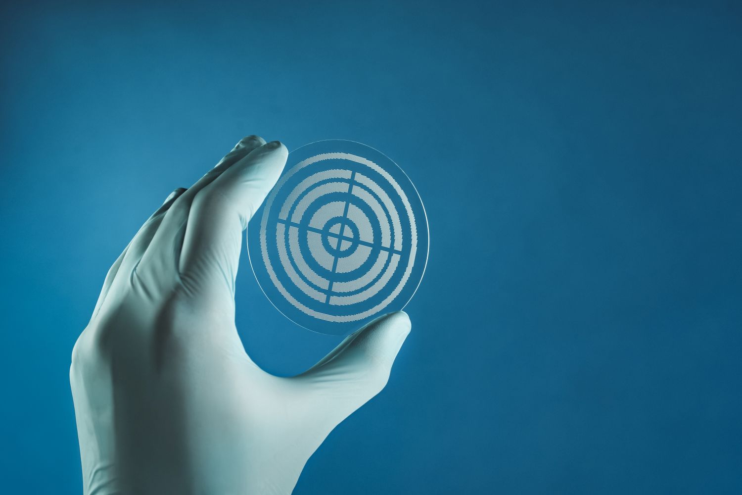
Our advanced processing capabilities enable us to provide ultra-high quality glass carrier wafers, glass spacers, interposers, TGV wafers, ceramic or glass guide plates for probe cards for the semiconductors industry.
Also, microfluidic chips and devices, multiwell plates, mesh filters, capillaries and needles micromachining, optical fibers processing, and laser marking on the surface of various materials for the biotech industry.
Our products Our servicesThe results, achieved using FemtoFBG present the stabilization of blue multi-emitter modules using fiber Bragg…
This EU-funded project is expected to revolutionize Green Energy Generation from photovoltaic panels across Europe.
WOP participates in the BILASURF project – a new European initiative to develop a solution…