

We provide glass drilling prototyping and production services for your designs.
We can works with your provided designs, o develop a prototype together.
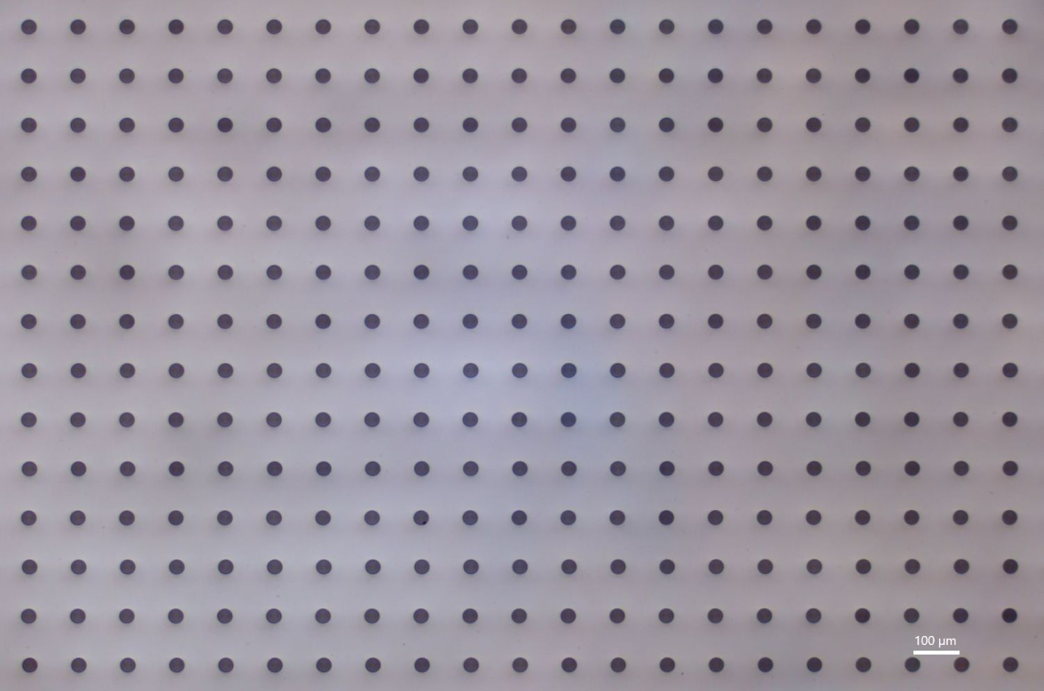
Glass drilling price depends on the type of glass chosen, design, number of pieces ordered.
For example, glass drilling of a wafer, holding 10000 to 3M holes per wafer, will cost from 0,00001 Eur per 1 hole (glass price is not included).
Rapid prototyping services to test your idea in an actual environment.
Small to medium scale production services from 1 unit. All materials.
Tailor-made laser systems designed for your specific applications.
Price from 0,75 Eur per hole.
Price from 0,01 Eur per hole.
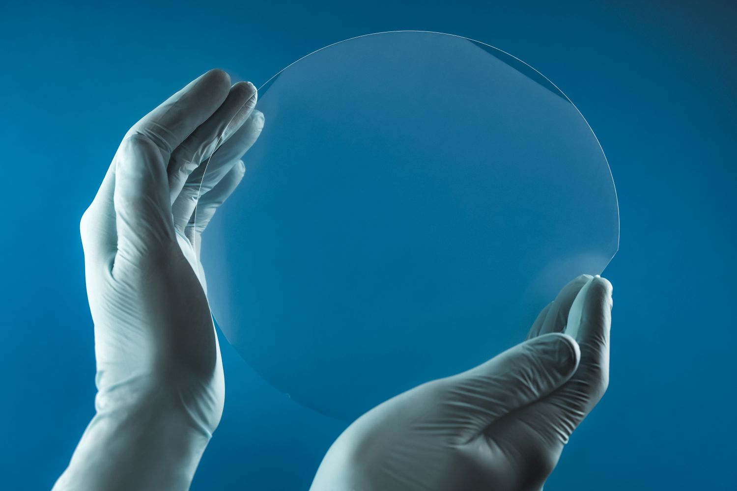
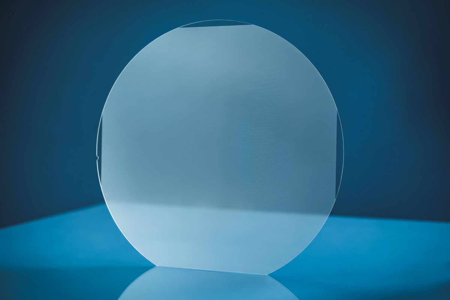
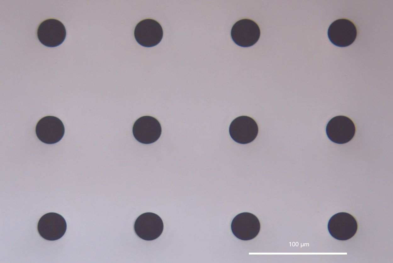
We offer ultra-high precision laser glass micro drilling. Highest quality in the market.
Glass & sapphire cutting and dicing workstation for industry, that outperforms other glass cutting methods.
WORKSHOP OF PHOTONICS
Mokslininku st. 6A, Vilnius, LT-08412, Lithuania
Phone: +370 5 215 7551
E-mail: [email protected]
Altechna R&D, UAB
Company code 301502628
VAT code LT100006155012
Bank – SEB 70440
LT87 7044 0600 0770 8092


